Altmemphy signals, Ddr2 and ddr sdram signals, Altmemphy signals –9 – Altera External Memory PHY Interface User Manual
Page 25: Ddr2 and ddr sdram signals –9
Chapter 3: Functional Description—ALTMEMPHY (nonAFI)
3–9
ALTMEMPHY Signals
© January 2010
Altera Corporation
External Memory PHY Interface (ALTMEMPHY) (nonAFI) Megafunction User Guide
ALTMEMPHY Signals
This section describes the ALMEMPHY megafunction signals for the following
interfaces:
■
DDR2 and DDR SDRAM signals
■
QDR II+ and QDR II SRAM signals
DDR2 and DDR SDRAM Signals
through
show the signals for DDR2 and DDR SDRAM nonAFIs.
The signal lists include the following signal groups:
■
I/O interface to the external memory device
■
Clock and reset signals
■
PLL reconfiguration signals
■
External DLL signals
■
User-mode calibrated on-chip termination (OCT) control signals
■
Interface to the memory controller
■
Local interface signals
■
Datapath interface for the controller
■
ALTMEMPHY megafunction calibration status interface
■
Additional calibration signals from the sequencer
1
Ports with the prefix “mem_” connect the PHY with the memory device; ports with the
prefix “ctl_” connect the PHY with the controller. Ports with prefix “ctl_mem_”
indicate the datapath for the controller; ports with the prefix “local_” indicate the
signal to be connected with the example driver or user logic.
1
Signals with suffix _n are active low; signals without suffix _n are active high.
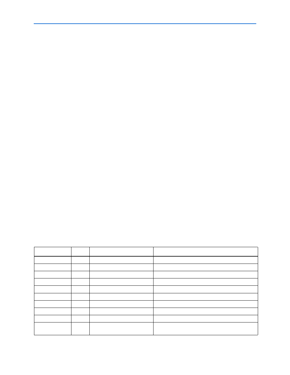
Table 3–1. I/O Interface for DDR2 and DDR SDRAM—nonAFI
(Part 1 of 2)
Signal Name
Type
Width
Description
mem_addr
output
MEM_IF_ROWADDR_WIDTH
The memory row and column address bus.
mem_ba
output
MEM_IF_BANKADDR_WIDTH
The memory bank address bus.
mem_cas_n
output
1
The memory column address strobe.
mem_cke
output
MEM_IF_CS_WIDTH
The memory clock enable.
mem_clk
bidir
MEM_IF_CLK_PAIR_COUNT
The memory clock, positive edge clock.
mem_clk_n
bidir
MEM_IF_CLK_PAIR_COUNT
The memory clock, negative edge clock.
mem_cs_n
output
MEM_IF_CS_WIDTH
The memory chip select signal.
mem_dm
output
MEM_IF_DM_WIDTH
The optional memory data mask bus.
mem_dq
bidir
MEM_IF_DWIDTH
The memory bidirectional data bus.
mem_dqs
bidir
MEM_IF_DWIDTH /
MEM_IF_DQ_PER_DQS
The memory bidirectional data strobe bus.