Altera External Memory PHY Interface User Manual
Page 59
Chapter 3: Functional Description—ALTMEMPHY (nonAFI)
3–43
Design Considerations
© January 2010
Altera Corporation
External Memory PHY Interface (ALTMEMPHY) (nonAFI) Megafunction User Guide
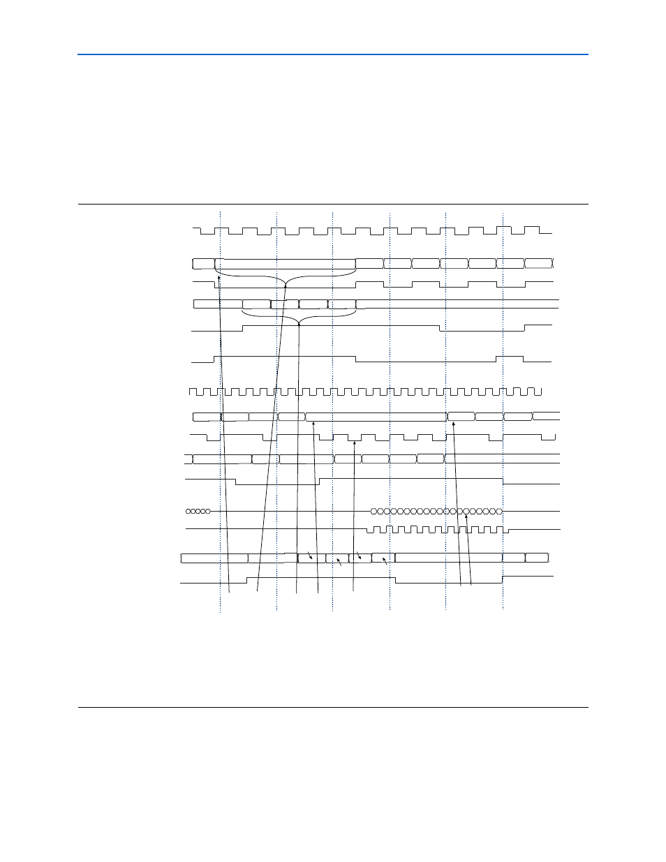
Handshake Mechanism Between Read Commands and Read Data
The controller generates a signal (ctl_doing_rd) to the ALTMEMPHY
megafunction which is asserted for one phy_clk cycle for every read command it
issues. If there are two read commands, the signal ctl_doing_rd is asserted for two
phy_clk
cycles. This signal also enables the capture registers and generates the
ctl_mem_rdata_valid
signal. This signal should be issued at the same time the
read command is sent to the ALTMEMPHY megafunction (refer to
1
The signals under the PHY Command Input label are the signals from the controller to
the ALTMEMPHY megafunction. The signals under the PHY Command Output label
are the signals coming out of the ALTMEMPHY megafunction and input to the
memory device.
Figure 3–12. Read Commands and Read Data (Half-Rate Controller)
Notes to
:
(1) The DDR command shows the command comprised of the command signals (ctl_mem_ras_n_h, ctl_mem_cas_n_h, and
ctl_mem_we_n_h)
seen at the ALTMEMPHY input. There can be more than one clock cycle of no operation (NOP) between active (ACT) to
RD depending on the value of t
RCD
parameter of your memory device.
(2) The DDR command shows the command comprised of the command signals (mem_ras_n_h, mem_cas_n_h and mem_we_n_h) seen at
the memory interface. There can be more than one clock cycle of NOP between active ACT to RD depending on the value of the t
RCD
parameter of
your memory device.
phy_clk
ctl_mem_addr_h
ctl_mem_cs_h
ctl_mem_odt_h
DDR Command
(1)
mem_clk
mem_addr
mem_odt
mem_dqs
mem_dq
ctl_mem_rdata
ctl_doing_rd
ctl_mem_rdata_valid
DDR Command
(2)
mem_cs_n
2818967... 503031e...
1
2
4
5
PHY Command Input
PHY Read Data Input
PHY Command Output
Memory Interface
PHY Read Data Output
2
3
4
NOP
NOP
NOP
NOP
RD
RD
PCH
ACT
NOP
0000
0004
0008
000C
0010
0000
PCH
NOP
NOP
NOP
NOP
ACT
PCH
RD
ACT
0000
0000
000C
0000
0010
0004
0008
0002
23eaf1c823eaf1c8 46c9ff8d...
8c8fe30...
0503db0...
0a06ab1...
140c4b3...
140c4b38140c4b38