Altera DDR SDRAM High-Performance Controllers and ALTMEMPHY IP User Manual
Page 57
Chapter 5: Functional Description—ALTMEMPHY
5–11
Block Description
June 2011
Altera Corporation
External Memory Interface Handbook Volume 3
Section I. DDR and DDR2 SDRAM Controllers with ALTMEMPHY IP User Guide
PLL Reconfiguration
The ALTMEMPHY parameter editor automatically generates the PLL reconfiguration
block by instantiating an ALTPLL_RECONFIG variation for Stratix II and
Stratix II GX devices to match the generated ALTPLL megafunction instance. The
ALTPLL_RECONFIG megafunction varies the resynchronization clock phase and the
measure clock phase.
1
The ALTMEMPHY parameter editor does not instantiate an ALTPLL_RECONFIG
megafunction for Arria II GX devices, as this device uses the dedicated phase
stepping I/O on the PLL.
DLL
A DLL instance is included in the generated ALTMEMPHY variation. When using the
DQS to capture the DQ read data, the DLL center-aligns the DQS strobe to the DQ
data. The DLL settings depend on the interface clock frequency.
f
For more information, refer to the External Memory Interfaces chapter in the device
handbook for your target device family.
Reset Management
The reset management block is responsible for the following:
■
Provides appropriately timed resets to the ALTMEMPHY megafunction datapaths
and functional modules
■
Performs the reset sequencing required for different clock domains
■
Provides reset management of PLL and PLL reconfiguration functions
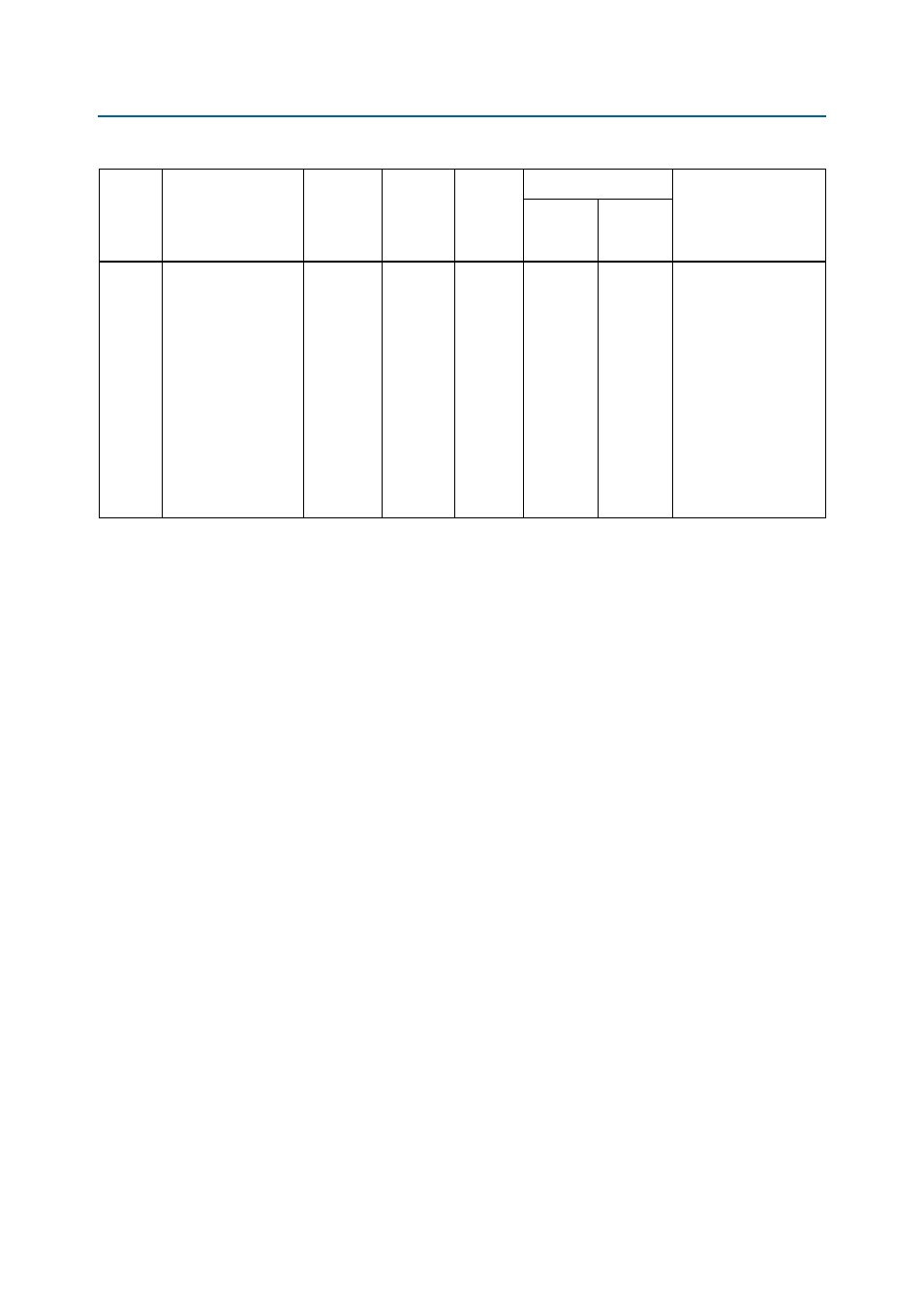
Half-rate
and full
rate
measure_clk_2x
C5
Calibrated
Full-Rate
Global
Regional
This clock is for VT
tracking. This
free-running clock
measures relative phase
shifts between the
internal clock(s) and
those being fed back
through a mimic path.
As a result, the
ALTMEMPHY
megafunction can track
VT effects on the FPGA
and compensate for the
effects.
Note to
Table 5–2
:
(1) In full-rate designs, a _1x clock may run at full-rate clock rate.
(2) The default clock network type is Global, however you can specify a regional clock network to improve clock jitter if your design uses any three
quadrants.
Table 5–2. DDR/DDR2 SDRAM Clocking in Arria II GX Devices (Part 3 of 3)
Design
Rate
Clock Name
(1)
Postscale
Counter
Phase
(Degrees)
Clock
Rate
Clock Network Type
Notes
All
Quadrants
Any 3
Quadrants
(2)