Partial write operations – Altera DDR SDRAM High-Performance Controllers and ALTMEMPHY IP User Manual
Page 92
5–46
Chapter 5: Functional Description—ALTMEMPHY
Using a Custom Controller
External Memory Interface Handbook Volume 3
June 2011
Altera Corporation
Section I. DDR and DDR2 SDRAM Controllers with ALTMEMPHY IP User Guide
The ctl_wlat signal is only valid when the calibration has been successfully
completed by the ALTMEMPHY sequencer and does not change at any point during
normal user mode operation.
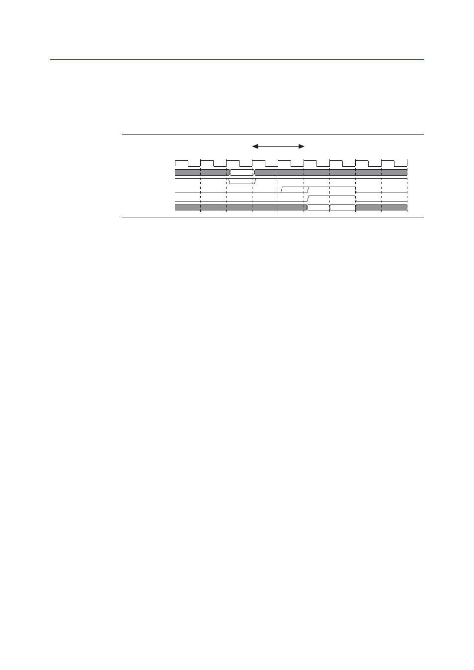
Figure 5–23
shows the operation of ctl_wlat port.
For a half-rate design ctl_cs_n is 2 bits, not 1. Also the ctl_dqs_burst and
ctl_wdata_valid
waveforms indicate a half-rate design. This write results in a burst
of 8 at the DDR. Where ctl_cs_n is driven 2'b01, the LSB (1) is the first value driven
out of mem_cs_n, and the MSB (0) follows on the next mem_clk. Similarly, for
ctl_dqs_burst
, the LSB is driven out of mem_dqs first (0), then a 1 follows on the next
clock cycle. This sequence produces the continuous DQS pulse as required. Finally,
the ctl_addr bus is twice MEM_IF_ADDR_WIDTH bits wide and so the address is
concatenated to result in an address phase two mem_clk cycles wide.
Partial Write Operations
As part of the DDR and DDR2 SDRAM memory specifications, you have the option
for partial write operations by asserting the DM pins for part of the write signal.
For designs targeting the Stratix III device families, deassert the ctl_wdata_valid
signal during partial writes, when the write data is invalid, to save power by not
driving the DQ outputs.
For designs targeting other device families, use only the DM pins if you require
partial writes. Assert the ctl_dqs_burst and ctl_wdata_valid signals as for full write
operations, so that the DQ and DQS pins are driven during partial writes.
The I/O difference between Stratix III device families and other device families makes
it only possible to use the ctl_dqs_burst signal for the DQS enable in Stratix III
devices.
Using a Custom Controller with the TimeQuest Timing Analyzer
The Report DDR command in the TimeQuest Timing Analyzer may return the
message Nothing to report when you use a custom controller.
To avoid this situation, you can edit your project’s QSF file and set the value of the
following line to On: set_global_assignment -name PROJECT_SHOW_ENTITY_NAME
Alternatively, you can perform the following procedure in the Quatrus II software
GUI:
1. On the Assignments menu, click Settings.
2. In the Category list, click Compilation Process Settings.
Figure 5–23. Timing for ctl_dqs_burst, ctl_wdata_valid, Address, and Command—Half-Rate
Design
ctl_clk
ctl_addr
ctl_cs_n
ctl_dqs_burst
ctl_wdata_valid
ctl_wdata
AdAd
AdAd
01
01
10
11
11
ctl_wlat = 2
1 2