Altera DDR SDRAM High-Performance Controllers and ALTMEMPHY IP User Manual
Page 74
5–28
Chapter 5: Functional Description—ALTMEMPHY
ALTMEMPHY Signals
External Memory Interface Handbook Volume 3
June 2011
Altera Corporation
Section I. DDR and DDR2 SDRAM Controllers with ALTMEMPHY IP User Guide
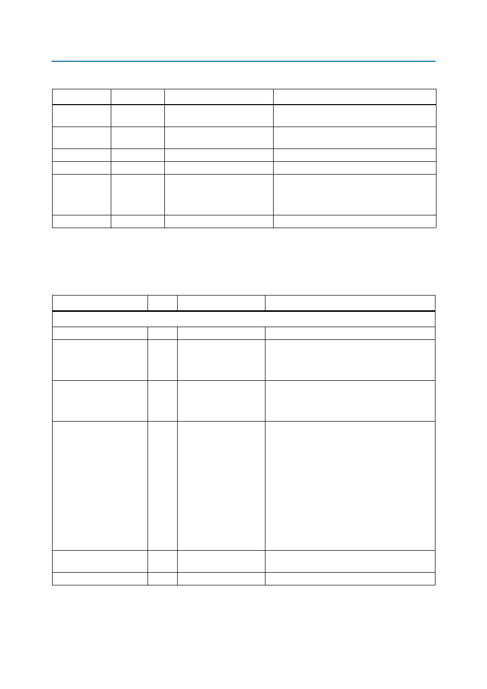
mem_dqs
Bidirectional
MEM_IF_DWIDTH/
MEM_IF_DQ_PER_DQS
The memory bidirectional data strobe bus.
mem_dqsn
Bidirectional
MEM_IF_DWIDTH/
MEM_IF_DQ_PER_DQS
The memory bidirectional data strobe bus.
mem_odt
Output
MEM_IF_CS_WIDTH
The memory on-die termination control signal.
mem_ras_n
Output
1
The memory row address strobe.
mem_reset_n
Output
1
The memory reset signal. This signal is derived
from the PHY’s internal reset signal, which is
generated by gating the global reset, soft reset, and
the PLL locked signal.
mem_we_n
Output
1
The memory write enable signal.
Notes to
Table 5–5
:
(1) Connected to I/O pads.
(2) Refer to
Table 5–8
for parameter description.
(3) Output is for memory device, and input path is fed back to ALTMEMPHY megafunction for VT tracking.
Table 5–5. Interface to the SDRAM Devices (Part 2 of 2)
(Note 1)
Signal Name
Type
Width
(2)
Description
Table 5–6. AFI Signals (Part 1 of 4)
Signal Name
Type
Width
(1)
Description
Clocks and Resets
pll_ref_clk
Input
1
The reference clock input to the PHY PLL.
global_reset_n
Input
1
Active-low global reset for PLL and all logic in the
PHY. A level set reset signal, which causes a complete
reset of the whole system. The PLL may maintain
some state information.
soft_reset_n
Input
1
Edge detect reset input intended for SOPC Builder use
or to be controlled by other system reset logic.
Causes a complete reset of PHY, but not the PLL used
in the PHY.
reset_request_n
Output
1
Directly connected to the locked output of the PLL
and is intended for optional use either by automated
tools such as SOPC Builder or could be manually
ANDed with any other system-level signals and
combined with any edge detect logic as required and
then fed back to the global_reset_n input.
Reset request output that indicates when the PLL
outputs are not locked. Use this as a reset request
input to any system-level reset controller you may
have. This signal is always low while the PLL is
locking (but not locked), and so any reset logic using
it is advised to detect a reset request on a falling-edge
rather than by level detection.
ctl_clk
Output
1
Half-rate clock supplied to controller and system
logic. The same signal as the non-AFI phy_clk.
ctl_reset_n
Output
1
Reset output on ctl_clk clock domain.