Stratix iii and stratix iv devices, Stratix iii and stratix iv devices –26 – Altera DDR SDRAM High-Performance Controllers and ALTMEMPHY IP User Manual
Page 72
5–26
Chapter 5: Functional Description—ALTMEMPHY
Block Description
External Memory Interface Handbook Volume 3
June 2011
Altera Corporation
Section I. DDR and DDR2 SDRAM Controllers with ALTMEMPHY IP User Guide
The DQ IOEs convert 2-n SDR bits to n-DDR bits.
The write datapath for full-rate PHYs is similar to the half-rate PHY. The IOE block is
identical to the half-rate PHY. The latency of the write datapath in the full-rate PHY is
less than in the half-rate PHY because the full-rate PHY does not have the
half-rate-to-full-rate conversion logic.
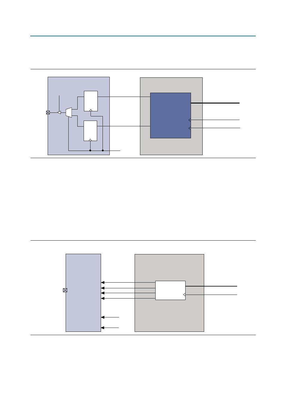
Stratix III and Stratix IV Devices
The memory controller interface outputs 4 n-bit wide data (ctl_wdata) at phy_clk_1x
frequency. The write data is clocked by the system clock phy_clk_1x at half data rate
and reordered into HDR of width 4 n-bits represented in
Figure 5–10
by
wdp_wdata3_1x, wdp_wdata2_1x, wdp_wdata1_1x
, and wdp_wdata0_1x.
All of the write datapath registers in the Stratix IV and Stratix III devices are clocked
by the half-rate clock, phy_clk_1x.
Figure 5–9. DDR/DDR2 SDRAM Write Datapath in Arria GX, Arria II GX, Cyclone III, HardCopy II, Stratix II, and Stratix II
GX Devices
Write Datapath
Stratix II IOE
wdp_wdata_l
phy_clk_1x (ctl_clk)
D
Q
D
Q
OE
DQ[n]
write_clk_2x
ctl_wdata[4n]
write_clk_2x
Data
Multiplexing
wdp_wdata_h
Figure 5–10. DDR and DDR2 SDRAM Write Datapath in Stratix IV and Stratix III Devices
Data
Ordering
Data Ordering
HDR to DDR
Conversion
mem_dq
Stratix III
IOE
write_clk_2x
phy_clk_1x
ctl_wdata[4n]
phy_clk_1x
wdp_wdata3_1x
wdp_wdata2_1x
wdp_wdata1_1x
wdp_wdata0_1x