Altera Arria 10 Avalon-ST User Manual
Page 219
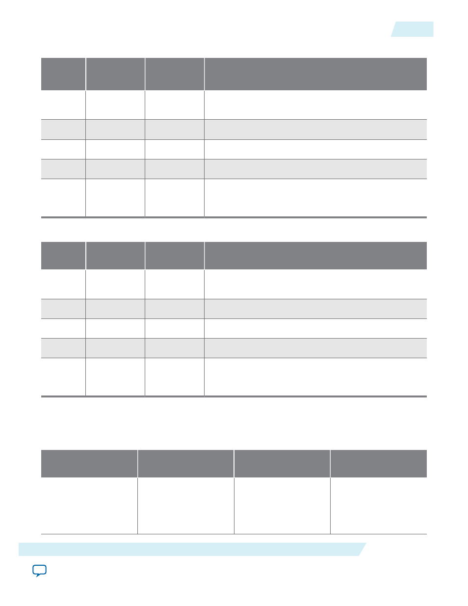
Table 17-16: Read Descriptor 1
Offset in BFM
Shared Memory
Value
Description
DW0
0x920
1,024
Transfer length in dwords and control bits as described in on
page 18–15
DW1
0x924
0
Endpoint address value
DW2
0x928
10
BFM shared memory data buffer 1 upper address value
DW3
0x92c
0x10900
BFM shared memory data buffer 1 lower address value
Data
Buffer 1
0x10900
Increment by 1
from 0xBBBB_
0001
Data content in the BFM shared memory from address:
0x10900
Table 17-17: Read Descriptor 2
Offset in BFM
Shared Memory
Value
Description
DW0
0x930
644
Transfer length in dwords and control bits as described in on
page 18–15
DW1
0x934
0
Endpoint address value
DW2
0x938
0
BFM shared memory upper address value
DW3
0x93c
0x20EF0
BFM shared memory lower address value
Data
Buffer 2
0x20EF0
Increment by 1
from 0xCCCC_
0001
Data content in the BFM shared memory from address:
0x20EF0
2. Sets up the chaining DMA descriptor header and starts the transfer data from the BFM shared memory
to the Endpoint memory by calling the procedure
dma_set_header
which writes four dwords,
DW0:DW3 into the DMA read register module.
Table 17-18: DMA Control Register Setup for DMA Read
Offset in DMA Control
Registers (BAR2)
Value
Description
DW0
0x0
3
Number of descriptors
and control bits as
described in Chaining
DMA Control Register
Definitions.
UG-01145_avst
2015.05.04
DMA Read Cycles
17-19
Testbench and Design Example
Altera Corporation