Altera ALTDLL User Manual
Page 43
4–7
Chapter 4: Functional Description
ALTDQ_DQS Megafunction
ALTDLL and ALTDQ_DQS Megafunctions User Guide
© February 2012
Altera Corporation
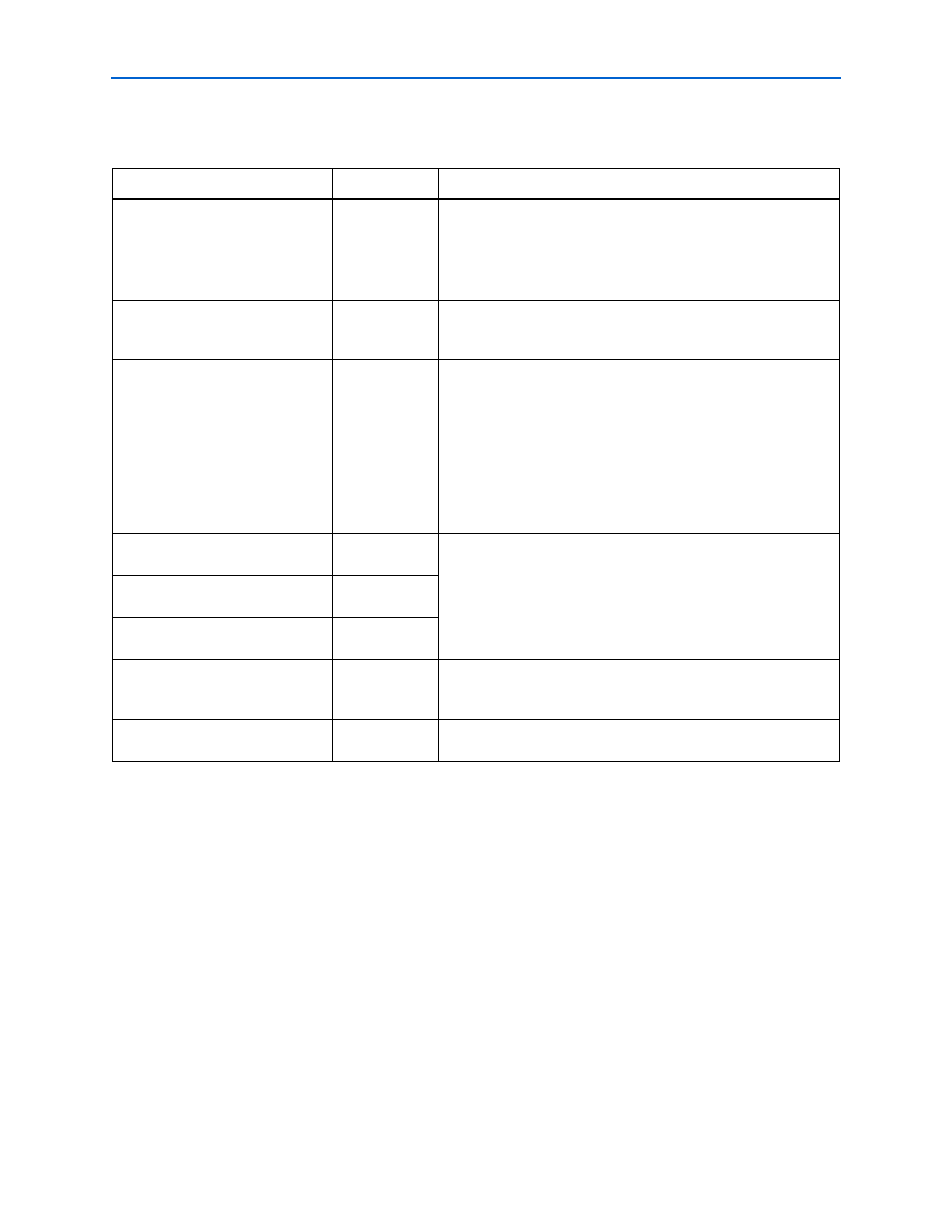
The DQS input path consists of the following blocks:
Table 4–3. DQS Input Path
Block
Name
Description
DQS_ENABLE_CTRL
DQS Enable
Control Block
Represents the circuitry to control the DQS enable block. Each DQS
enable block can be controlled by a DQS enable control block.
For more information about the DQS enable control, refer to the
DQS Postamble Circuitry section in the External Memory Interface
chapter of the respective device handbooks.
DQS_ENABLE_CTRL_HR_DDIO
_OUT
DQS Enable
Control Half
Rate Block
Represents the circuitry to transfer input to the
DQS_ENABLE_CTRL block
from a half-rate clock to a full-rate
clock.
DQS_ENABLE
DQS Enable
Block
Represents the AND-gate control on the DQS input used to ground
the DQS input strobe when the strobe goes to Z after a DDR read
postamble. The
DQS_ENABLE
block enables the registers to allow
enough time for the DQS delay settings to travel from the DQS
phase-shift circuitry or core logic to all the DQS logic blocks before
the next change.
For more information about the DQS enable block, refer to the
Update Enable Circuitry section in the External Memory Interfaces
chapter of the respective device handbooks.
DQS_DELAY_CHAIN
DQS Delay
Chain Block
For more information about these delay chains, refer to
DQSBUSOUT_DELAY_CHAIN
DQS Busout
Delay Chain
DQS_ENABLE_DELAY_CHAIN
DQS Enable
Delay Chain
DQS_CONFIG
DQS
Configuration
Blocks
For more information about
DQS_CONFIG
block, refer to
.
IO_CLOCK_DIVIDER
I/O Clock
Divider Block
For more information about I/O clock divider block, refer to
.