Dq input path, Dq input path –8 – Altera ALTDLL User Manual
Page 44
Chapter 4: Functional Description
4–8
ALTDQ_DQS Megafunction
© February 2012
Altera Corporation
ALTDLL and ALTDQ_DQS Megafunctions User Guide
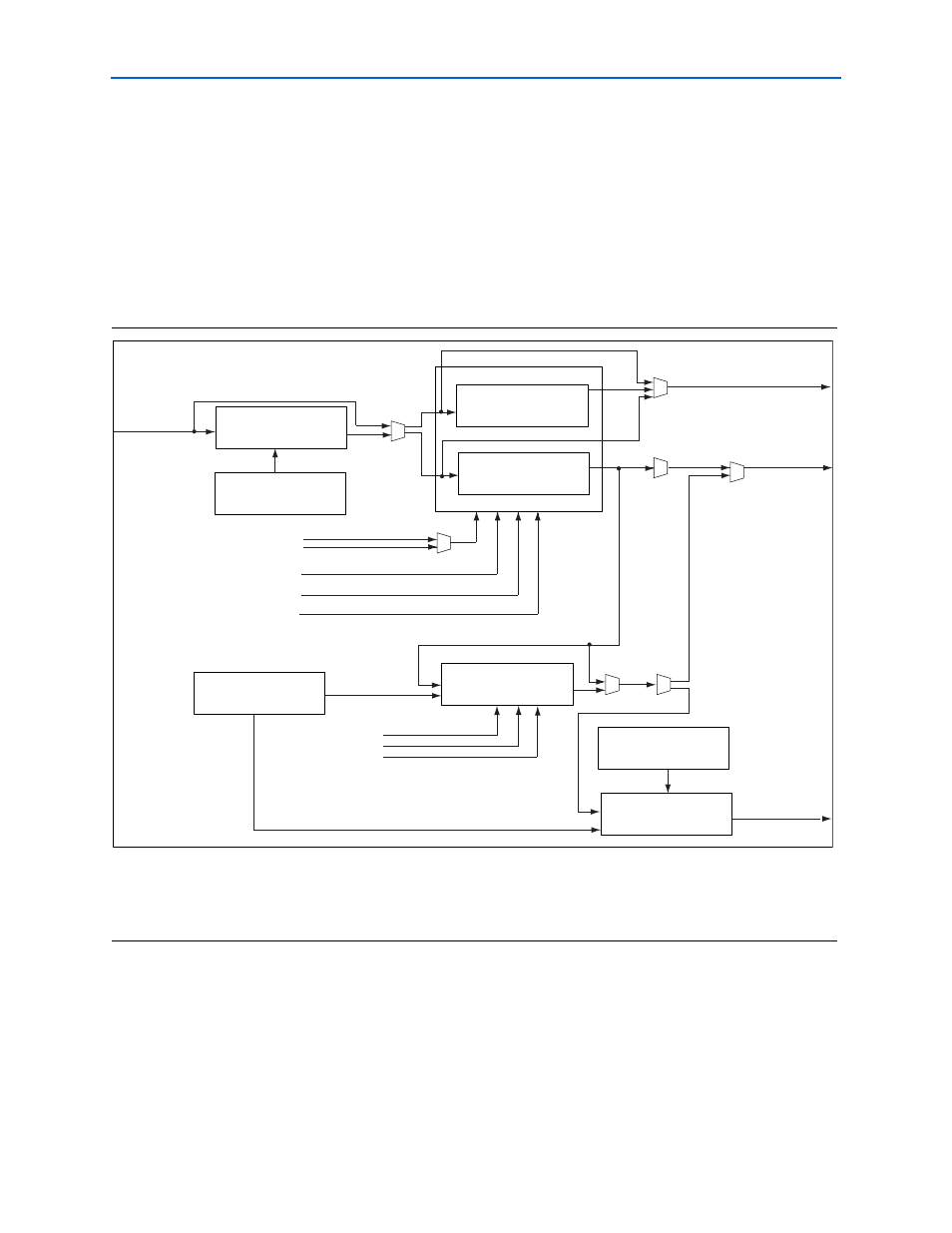
DQ Input Path
This path receives the DQ signal from the external memory during read operations.
Instantiate this path for all input-only and bidirectional DQ I/O pins.
shows the available blocks in the DQ input path and the connections with the
ALTDQ_DQS ports.
1
The value for <IO> depends on your selection in the parameter editor. The possible
values are
BIDIR_DQ
and
INPUT_DQ
.
Figure 4–4. DQ Input Path
,
Notes to
(1) The <IO>
_input_data_in
port must be connected to the output port of the input buffer.
(2) The
dll_delayctrlin
port must be connected to the DLL.
(3) The
IO_CLOCK_DIVIDER
, <IO>
_HALF_RATE_INPUT
, <IO>
_IPA_LOW
, and <IO>
_IPA_HIGH
blocks are half-rate components.
<IO>_INPUT_DELAY_CHAIN (D1)
<IO>_INPUT_FF
<IO>_DDIO_IN
<IO>_IPA_LOW and <IO>_IPA_HIGH
dq_input_reg_clk
dqs_bus
dqs_input_reg_clkena
<io>_areset
<io>_sreset
DQS_CONFIG
<IO>_CONFIG
<IO>_HALF_RATE_INPUT
<IO>_hr_input_data_out
dq_ipa_clk
dll_delayctrlin
<io>_sreset
IO_CLOCK_DIVIDER
<IO>_input_data_out_low
<IO>_input_data_out_high
<IO>_input_data_out
<IO>_input_data_in
and
DQ Input Path