Altera ALTDLL User Manual
Page 49
4–13
Chapter 4: Functional Description
ALTDQ_DQS Megafunction
ALTDLL and ALTDQ_DQS Megafunctions User Guide
© February 2012
Altera Corporation
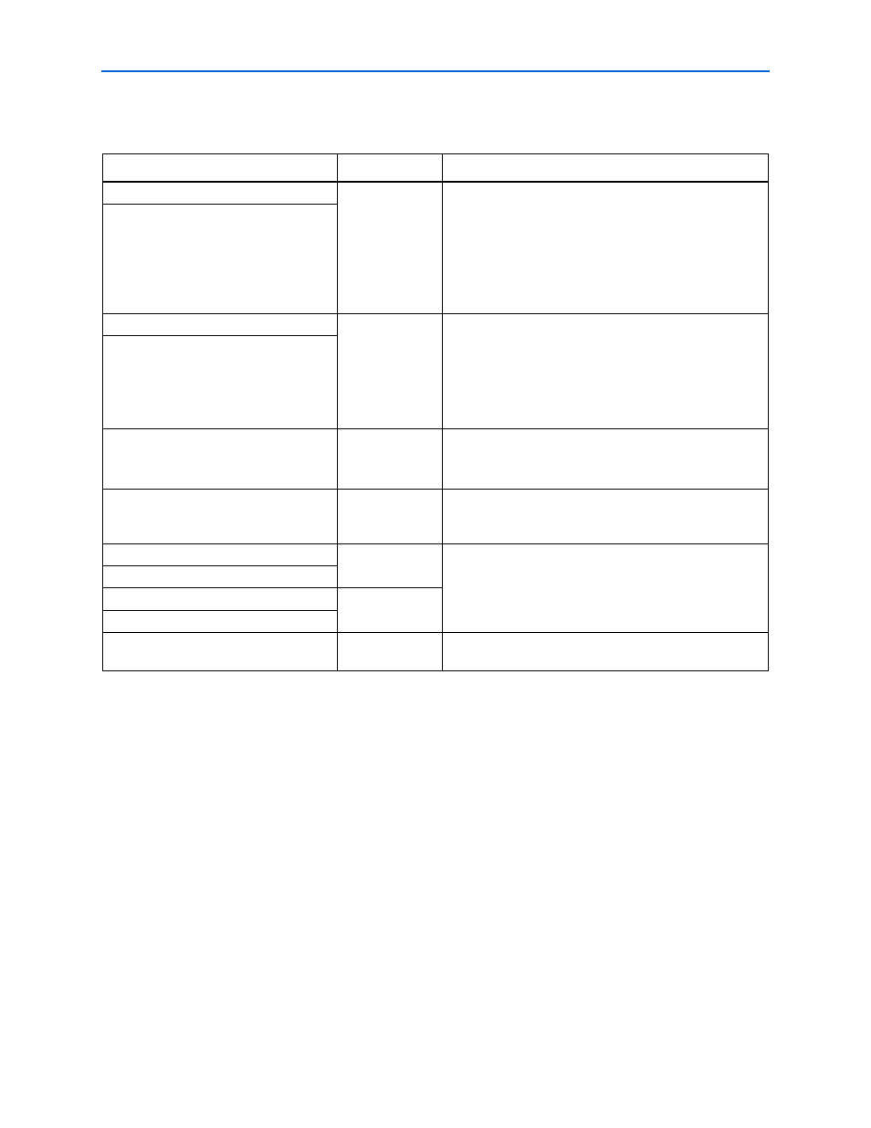
The DQS output and OE path consist of the following blocks:
Table 4–6. DQS Output and OE Path
Block
Name
Description
DQS_OUTPUT_FF
DQS output
register blocks
Sends data directly to the external memory DQs pins
during a write operation through the output buffer. These
blocks are clocked by the DQS write clock.
The
DQS_OUTPUT_FF
block represents a group of
flip-flop registers in the DQS output path.
The
DQS_OUTPUT_DDIO_OUT
represents a group of
double data rate output registers in the DQS output path.
DQS_OUTPUT_DDIO_OUT
DQS_OE_FF
DQS output
enable register
blocks
Sends output enable signal to the output buffer. These
blocks are clocked by the DQS write clock.
The
DQS_OE_FF
block represents a group of flip-flop
registers in the DQS OE path.
The
DQS_OE_DDIO_OE
represents a group of double
data rate registers in the DQS OE path.
DQS_OE_DDIO_OE
DQS_OUTPUT_HR_DDIO_OUT_HIGH
and
DQS_OUTPUT_HR_DDIO_OUT_LOW
Half-rate output
register block
Represents the DDIO registers that are used to transfer
DQS signals from the core during half-rate write operation.
These blocks are clocked by the DQS write clock.
DQS_OE_HR_DDIO_OUT
Half-rate output
enable register
block
Represents the DDIO registers that are used to transfer
half-rate DQS output enable signals to the output buffer.
DQS_OUTPUT_DELAY_CHAIN1
(D5)
DQS output delay
chains
For more information about the DQS output and OE delay
chains, refer to
.
DQS_OUTPUT_DELAY_CHAIN2
(D6)
DQS_OE_DELAY_CHAIN1
(D5)
DQS OE delay
chains
DQS_OE_DELAY_CHAIN2
(D6)
IO_CONFIG
I/O Configuration
Block
For more information about the
IO_CONFIG
block, refer
.