Avago Technologies LSI53C1000R User Manual
Page 280
5-38
SCSI SCRIPTS Instruction Set
Version 2.2
Copyright © 2000–2003 by LSI Logic Corporation. All rights reserved.
A maximum of 4 bytes may be moved with these instructions. The
register address and memory address must have the same byte
alignment, and the count set such that it does not cross Dword
boundaries. The memory address may not map back to the chip,
excluding RAM and ROM. If it does, a PCI read/write cycle occurs
(the data does not actually transfer to/from the chip), and the chip issues
an interrupt (Illegal Instruction Detected) immediately following.
The SIOM and DIOM bits in the
register determine
whether the destination or source address of the instruction is in
Memory space or I/O space, as illustrated in the following table. The
Load/Store utilizes the PCI commands for I/O read and I/O write to
access the I/O space.
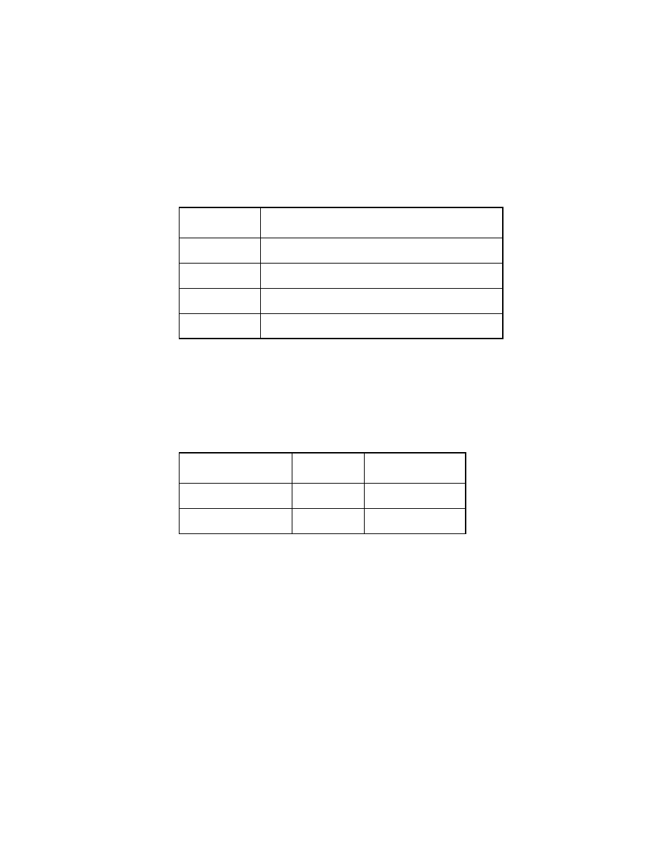
Bits A1, A0
Number of Bytes Allowed to Load/Store
00
One, two, three or four
01
One, two, or three
10
One or two
11
One
Bit
Source
Destination
SIOM (Load)
Memory
Register
DIOM (Store)
Register
Memory