Operating register/scripts ram write, 64 bits – Avago Technologies LSI53C1000R User Manual
Page 305
Advertising
PCI and External Memory Interface Timing Diagrams
6-23
Version 2.2
Copyright © 2000–2003 by LSI Logic Corporation. All rights reserved.
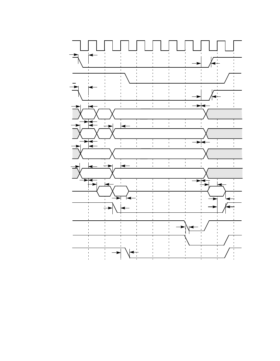
Figure 6.16 Operating Register/SCRIPTS RAM Write, 64 Bits
Byte Enable
t
2
t
1
t
2
t
1
t
2
t
1
t
2
t
2
t
3
t
2
t
1
t
3
CLK
(Driven by System)
FRAME/
(Driven by Master)
AD[31:0]
(Driven by Master)
C_BE[3:0]/
(Driven by Master)
PAR; PAR64
(Driven by Master)
IRDY/
(Driven by Master)
TRDY/
(Driven by LSI53C1000R)
STOP/
(Driven by LSI53C1000R)
DEVSEL/
(Driven by LSI53C1000R)
In
In
t
1
t
2
Addr
Lo
Addr
Hi
t
1
Dual
Addr
t
1
AD[63:32]
(Driven by Master)
Hi Addr
Byte Enable
t
2
C_BE[7:4]/
(Driven by Master)
t
1
Bus CMD
t
1
t
2
Bus
CMD
In
REQ64/
(Driven by Master)
ACK64/
(Driven by LSI53C1000R)
Data In
t
2
t
1
t
2
t
1
Data In
Advertising
This manual is related to the following products: