3 block diagram – Watson-Marlow MM420 User Manual
Page 56
Advertising
3 Functions
Issue 10/06
MICROMASTER 420 Operating Instructions
56
6SE6400-5AA00-0BP0
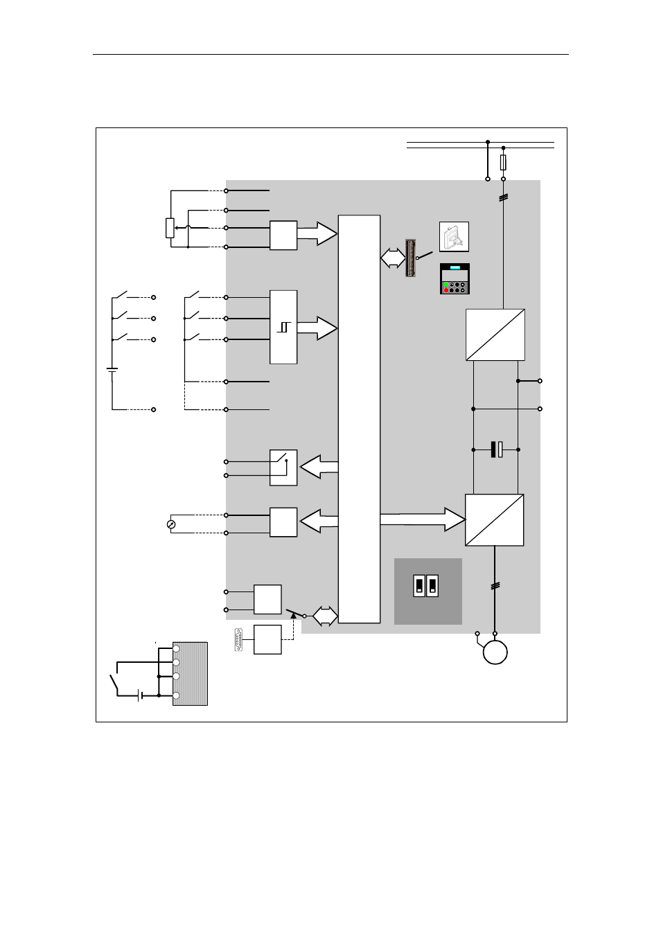
3.3 Block
diagram
PE
1/3 AC 200 - 240 V
3 AC 380 - 480 V
SI
PE
L/L1, N/L2
L/L1, N/L2, L3
L1, L2, L3
=
3 ~
PE
U,V,W
M
A/D
+10 V
0 V
0 - 20 mA
max. 500
Ω
CPU
RS485
D/A
~
=
ADC+
ADC-
DIN1
DIN2
DIN3
DAC+
DAC-
P+
N-
RL1-B
RL1-C
1
2
3
4
5
6
7
8
9
12
13
14
15
10
11
≥ 4.7 kΩ
Output 0 V
max. 100 mA
(isolated)
30 V DC / 5 A (resistive)
250 V AC / 2 A (inductive)
Relay
Output +24 V
max. 100 mA
(isolated)
D
C
-li
nk c
onn
ec
tion
or
or
CB
Option
automatic
DC+
DC
−
DIN4
2
3
4
9
24 V
-
+
The analog input circuit can be
alternatively configured to
provide an additional digital
input (DIN4):
1
2
60 Hz
50 Hz
DIP switch
Not
used
BOP link
COM link
Jog
0
I
P
Fn
Hz
150.00
BOP/AOP
RS232
DIN1
DIN2
DIN3
5
6
7
9
External 24 V
NPN
PNP
or
24 V
+
_
Fig. 3-11
MICROMASTER 420 – block diagram
Advertising