Altera POS-PHY Level 4 IP Core User Manual
Page 48
4–10
Chapter 4: Functional Description—Receiver
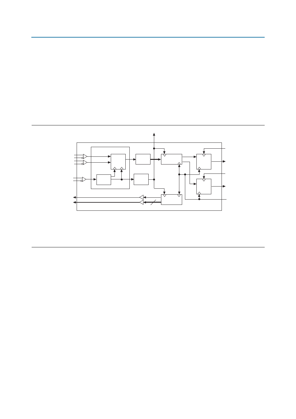
Clock Structure
POS-PHY Level 4 IP Core User Guide
December 2014
Altera Corporation
In multiple clock domain mode, an input clock is instantiated for each Atlantic FIFO
buffer in the IP core, which is used for the read side of the buffers. The naming
convention for these input clocks is aN_arxclk. These clocks are inputs to the IP core
and can either be tied together or controlled individually. No specific frequency
requirement is specified for the aN_arxclk clocks, but they should be fast enough to
ensure that the FIFO buffers do not fill, otherwise backpressure is asserted via the SPI-
4.2 status channel.
Figure 4–4 on page 4–10
shows the multiple clock domain clocking structure for the
receiver IP core, for 128- and 64-bit individual buffers variations. For shared buffer
with embedded addressing variations, only Atlantic buffer port 0 is instantiated.
Figure 4–4. Clock Layout Diagram (Full Rate)
Notes to
Figure 4–4
:
(1) Stratix GX 64-bit DPA only.
(2) The single clock mode removes the separate Atlantic clocks.
(3) The embedded address mode has only one buffer; the individual buffers mode can have more than one buffer.
(4) The rsclk in 128-bit data path source is rdint_clk. 64-bit is internally generated (status processor).
Channel
Aligner
DPA/
SERDES
LVDS
PLL
LVTTL
LVTTL
EPLL
(Note 1)
Status
Processor
Data
Processor
Atlantic
Buffer 0
Atlantic
Interface 0
a0_arxclk
aN_arxclk
(Note 2, 3)
rdclk
rdat[15:0]
rctl
rxsys_clk
rdint_clk
altlvds Megafunction
rsclk (Note 4)
rstat[1:0]
Atlantic
Buffer N
Atlantic
Interface N
2