2 v.35 interface, 2 specification – Comtech EF Data SDM-100A User Manual
Page 134
Theory of Operation
SDM-100A Satellite Modem
4–18
Rev.
0
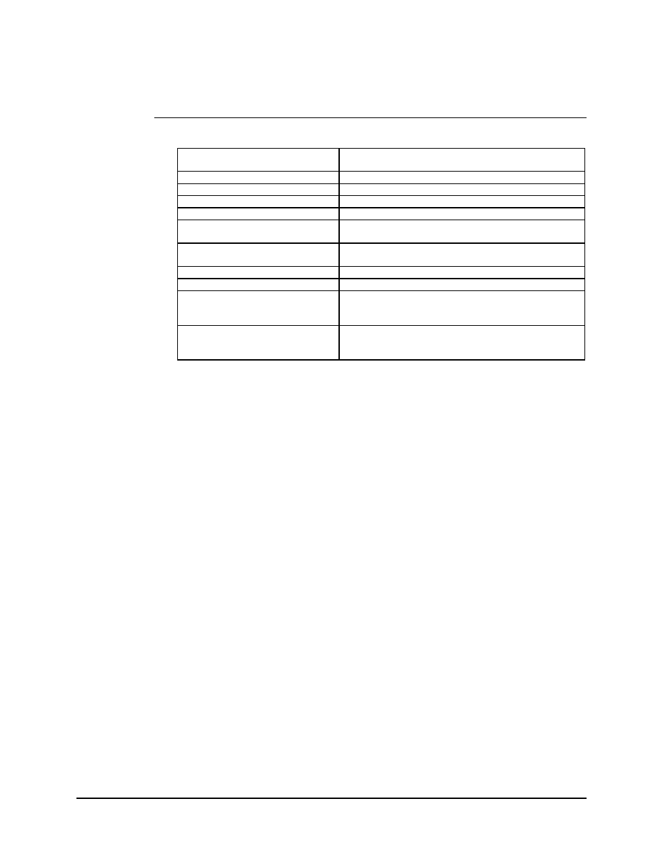
4.4.1.2 Specification
Circuit Supported
SD, ST, TT, RD, RT, DM, RR, MC, MOD FAULT,
DEMOD FAULT
Amplitude (RD, RT, ST, DM, RR)
4,
±
2V differential into 100
Ω
DC Offset (RD, RT, ST, DM, RR)
0.0,
±
0.4V
Impedance (RD, RT, ST, DM, RR)
Less than 100
Ω
, differential
Impedance (SD, TT, MC)
100,
±
20
Ω
, differential
Polarity
True when B positive with respect to A
False when A positive with respect to B
Phasing (RD, RT)
False-to-True transition of RT nominally in center of RD
data bit
Symmetry (ST, TT, RT)
50%,
±
5%
Frequency Stability (ST)
±
100 PPM
Modulator Fault
Open collector output
15V max, 20 mA max current sink
Fault is open circuit
Demodulator Fault
Open collector output
15V max, 20 mA max current sink
Fault is open circuit
4.4.2 V.35 Interface
The V.35 digital interface provides level translation, buffering, and termination between
the internal modem signals and the V.35 DCE interface on the rear panel. Electrical
characteristics of the interface signals are defined in CCITT Recommendation V.35. The
electrical and mechanical specifications are summarized in Sections 4.4.2.1 and 4.4.2.2.
Refer to Figure 4-7 for a functional block diagram of the interface.
The V.35 interface provides a Serial Clock Transmit (SCT) clock signal at the modem
data rate.
• In the INTERNAL clock mode, the data to be transmitted, Send Data (SD), must
be synchronized to SCT.
• In the EXTERNAL clock mode, the clock is accepted on the Serial Clock
Transmit External (SCTE) input to clock-in the data to be transmitted.
In either case, the phase relationship between the clock and data is not important, as long
as it meets the jitter specification. This is because a clock phase correction circuit is
provided, which shifts the clock away from the data transition times.