Clock diagrams for most cpri ip core variations, Clock diagrams for most cpri ip core variations –6, Figure 4–2 on – Altera CPRI IP Core User Manual
Page 38: Figure 4–2
4–6
Chapter 4: Functional Description
Clocking Structure
CPRI MegaCore Function
December 2013
Altera Corporation
User Guide
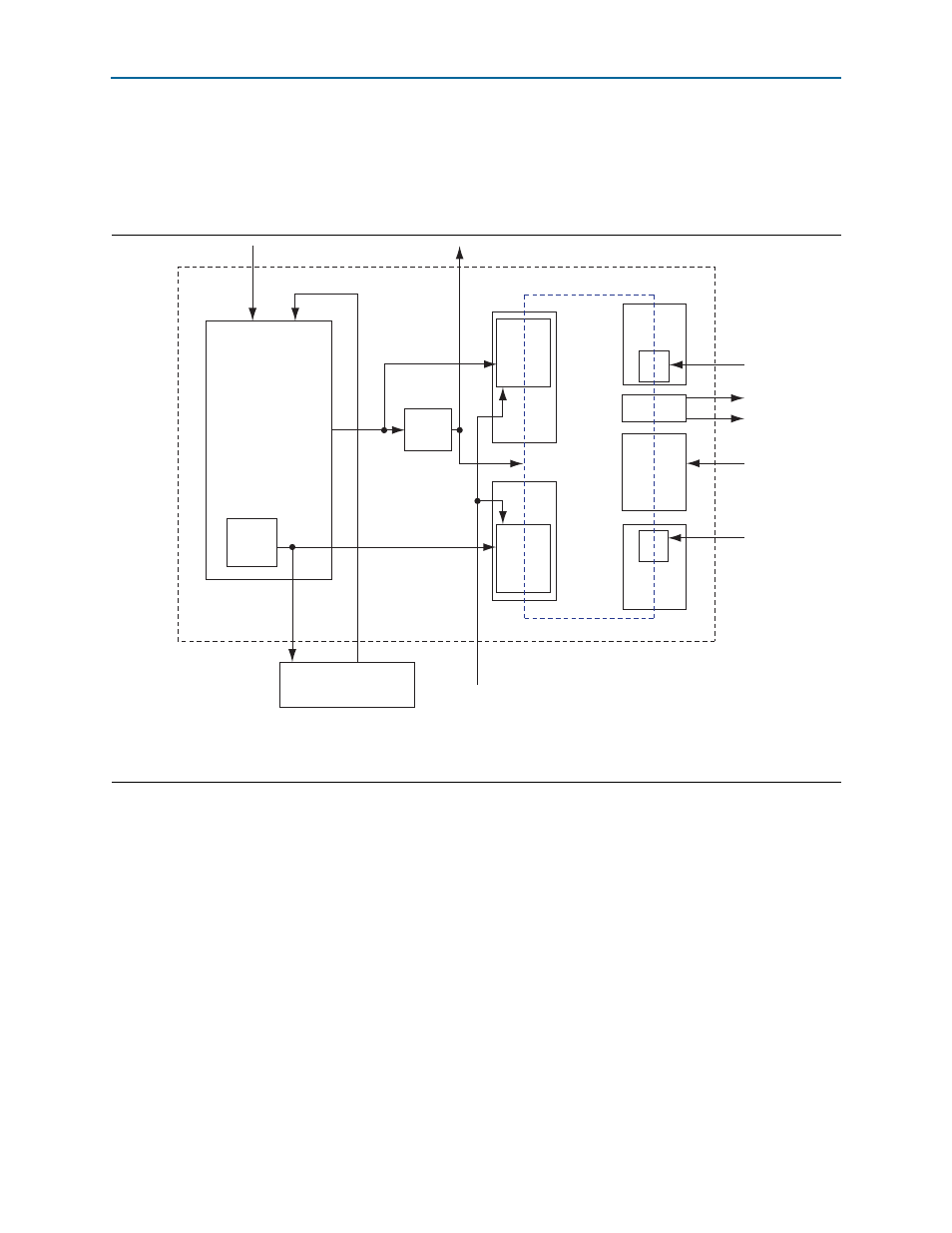
Clock Diagrams for Most CPRI IP Core Variations
shows the clock diagram for a CPRI IP core configured as an RE slave,
unless the IP core is configured with CPRI line rate 9.830.4 Mbps and targets an
Arria V GT device.
Figure 4–2. CPRI IP Core Slave Clocking Except for Arria V GT 9.8 Gbps Variations
Note to
(1) The clock divider factor depends on the device family. In device families with a factor of 1, the divider is not configured.
Table 4–17 on page 4–59
lists the datapath width and clock divider by device family.
Transceiver
CPRI TX
MII Interface
CPU
Interface
Rx Elastic
Sync Buffer
Tx Elastic
Sync Buffer
CPRI RX
CDR
FIFO
Buffer
CPRI MegaCore Function
Clock
Divider
(1)
Clean-Up PLL
cpu_clk
gxb_pll_inclk
pll_clkout
tx_clkout
cpri_clkout
cpri_clkout
Clock
Domain
rx_clkout
gxb_refclk
mapN_tx_clk
clk_ex_delay
FIFO
Buffer
mapN_rx_clk
CPRI Rx
MAP
Interface
CPRI Tx
MAP
Interface
cpri_mii_txclk
cpri_mii_rxclk