Figure 4–3 – Altera CPRI IP Core User Manual
Page 39
Chapter 4: Functional Description
4–7
Clocking Structure
December 2013
Altera Corporation
CPRI MegaCore Function
User Guide
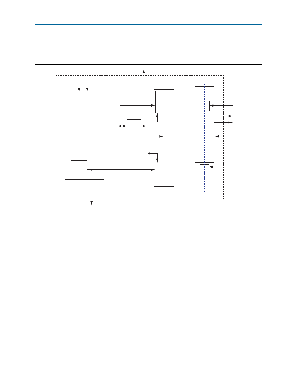
shows the clock diagram for a CPRI IP core configured as an REC master
or as an RE master, unless the IP core is configured with CPRI line rate 9830.4 Mbps
and targets an Arria V GT device.
Clock Diagrams for CPRI IP Core Arria V GT Variations at 9830.4 Mbps
CPRI IP core variations configured with a CPRI line rate of 9830.4 Mbps that target an
Arria V GT device have a different clocking scheme. These variations have no clock
divider, and have neither an RX elastic buffer nor a TX elastic buffer.
These variations use two additional input clock signals,
usr_clk
and
usr_pma_clk
.
describes the requirements for these two input clock signals.
When a variation configured with a CPRI line rate of 9830.4 Mbps that targets an
Arria V GT device participates in autorate negotiation, you must modify the
frequency of the
usr_clk
and
usr_pma_clk
input clocks to specific values for the
different CPRI line rates. Refer to
Appendix B, Implementing CPRI Link Autorate
Figure 4–3. CPRI IP Core Master Clocking Except for Arria V GT 9.8 Gbps Variations
Note to
(1) The clock divider factor depends on the device family. In device families with a factor of 1, the divider is not configured.
Table 4–17 on page 4–59
lists the datapath width and clock divider by device family.
Transceiver
CPRI TX
MII Interface
CPU
Interface
Rx Elastic
Sync Buffer
Tx Elastic
Sync Buffer
CPRI RX
CDR
FIFO
Buffer
CPRI MegaCore Function
Clock
Divider
(1)
cpu_clk
gxb_pll_inclk
pll_clkout
tx_clkout
cpri_clkout
cpri_clkout
Clock
Domain
rx_clkout
gxb_refclk
mapN_tx_clk
clk_ex_delay
FIFO
Buffer
mapN_rx_clk
CPRI Rx
MAP
Interface
CPRI Tx
MAP
Interface
cpri_mii_txclk
cpri_mii_rxclk