Altera Cyclone II DSP Development Board User Manual
Page 103
Advertising
Altera Corporation
Reference Manual
C–17
August 2006
Cyclone II DSP Development Board
GND
P16
P23
DAC_B_D7
GND
P18
P24
EVM_D27
GND
P19
P25
EVM_RESET
GND
P20
P26
EVM_AREN
GND
P8
P3
DAC_A_D10
GND
P9
P4
VGA_R6
GND
R1
P5
3.3V
GND
R12
P6
DAC_A_D13
GND
R13
P7
DIG_LSB_DP
GND
R14
P8
GND
GND
R15
P9
GND
GND
R17
R1
GND
GND
R21
R10
1.2V
GND
R26
R11
1.2V
GND
T10
R12
GND
GND
T12
R13
GND
GND
T13
R14
GND
GND
T14
R15
GND
GND
T15
R16
1.2V
GND
T17
R17
GND
GND
T5
R18
3.3V
GND
U10
R19
1.2V
GND
U12
R2
ADC_B_OE
GND
U17
R20
PROTO_CLKIN
GND
U19
R21
GND
GND
U8
R22
EP2C_STATUSN
GND
V11
R23
EP2C_CONFIG_DONE
GND
V13
R24
EVM_D25
GND
V14
R25
SRAM_CLK
GND
V17
R26
GND
GND
W12
R3
VGA_G0
GND
W13
R4
AUDIO_SCLK
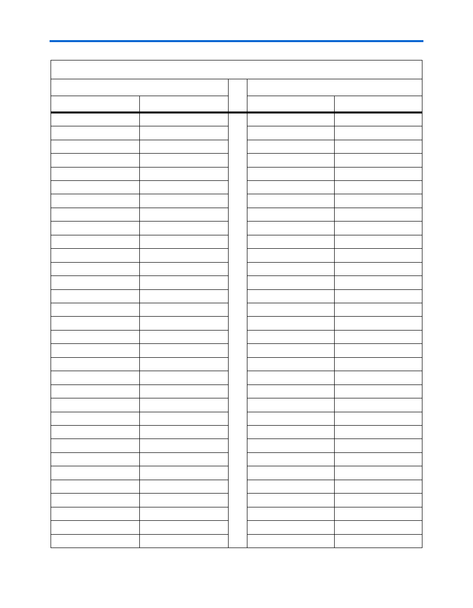
Table C–1. Cyclone II EP2C70F672-C6ES FPGA Pin-Outs (Part 17 of 22)
Note (1)
Alphabetical by Signal Name
Alphabetical by Pin Number
Schematic Signal Name
Pin Number
Pin Number
Schematic Signal Name
Advertising