Altera Cyclone II DSP Development Board User Manual
Page 52
2–44
Reference Manual
Altera Corporation
Cyclone II DSP Development Board
August 2006
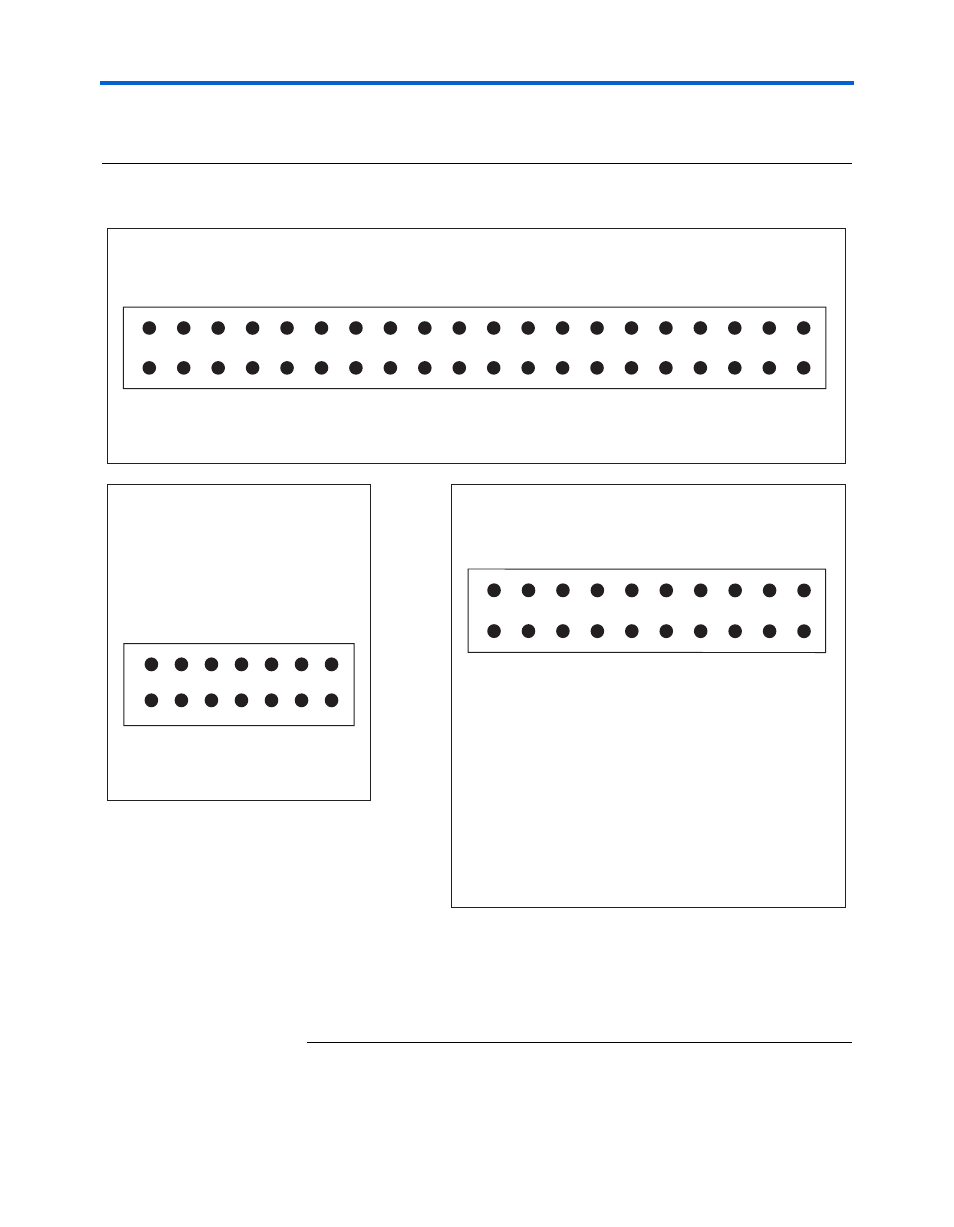
Expansion Connectors
shows the Expansion Prototype Connector pin numbers.
Figure 2–16. Expansion Prototype Connector Pin Numbers - J15, J22 & J23
Notes to
(1)
Voltage from DC power supply.
(2)
Clock from the clock buffer U16.
(3)
Clock from the EP2C70.
(4)
Clock output from the card connected to the Expansion Prototype Connector.
J15
A14
J5
G6
L6
K7
G5
G4
C2
D1
GND
G1
J3
H1
J1
K1
L2
M2
K3
G2
E2
GND
H6
F6
L7
J8
F4
G3
F2
F1
NC
GND
GND
GND
J2
GND
M3
NC
H3
V2
GND
1
3
5
7
9
11
13
15
17
19
21
23
25
27
29
31
33
35
37
39
2
4
6
8
10
12
14
16
18
20
22
24
26
28
30
32
34
36
38
40
J23
(1)
DC_INPUT
NC
3.3V
3.3V
(2)
PR
O
T
O_CLK_OSC
(U16 Pin 5)
(3)
PR
O
T
O_CLKIN (R20)
(4)
PR
O
T
O_CLK
OUT (
AD13)
3.3V
3.3V
3.3V
GND
GND
GND
GND
GND
GND
GND
GND
GND
GND
1
3
5
7
9
11
13
15
17
19
2
4
6
8
10
12
14
16
18
20
J22
GND
C3
L3
K5
H4
L4
K6
PR
O
T
O_3_3V_5V
D2
J7
J4
K4
J6
K8
1
3
5
7
9
11
13
2
4
6
8
10
12
14