Altera Cyclone II DSP Development Board User Manual
Page 49
Advertising
Altera Corporation
Reference Manual
2–41
August 2006
Cyclone II DSP Development Board
Cyclone II DSP Development Board Components
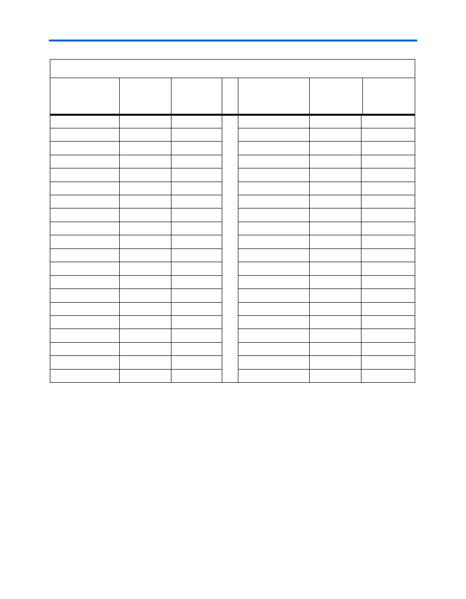
CE1_n
98
J24
VDDQ
4
CE2
97
VDDQ
11
CE3_n
92
AE25
VDDQ
20
CLK
89
R25
VDDQ
27
DQA0
52
G24
VDDQ
54
DQA1
53
G23
VDDQ
61
DQA2
56
H24
VDDQ
70
DQA3
57
H23
VDDQ
77
DQA4
58
J23
VSS
17
DQA5
59
J22
VSS
40
DQA6
62
K23
VSS
67
DQA7
63
K22
VSS
90
DQB10
72
L21
VSSQ
5
DQB11
73
L19
VSSQ
10
DQB12
74
M20
VSSQ
21
DQB13
75
N20
VSSQ
26
DQB14
78
M19
VSSQ
55
DQB15
79
V22
VSSQ
60
DQB8
68
K21
VSSQ
71
DQB9
69
K19
VSSQ
76
Note to
(1)
Blank cells indicate no connection.
Table 2–23. SSRAM Device Pin-Outs (Part 2 of 2)
Note (1)
SSRAM Pin Name
SSRAM (U22)
Pin Number
Cyclone II
(U12) Pin
Number
SSRAM Pin Name
SSRAM (U22)
Pin Number
Cyclone II
(U12) Pin
Number
Advertising