Clk sma connector (j17), U16). (see, Table 2–31 – Altera Cyclone II DSP Development Board User Manual
Page 69
Altera Corporation
Reference Manual
2–61
August 2006
Cyclone II DSP Development Board
Cyclone II DSP Development Board Components
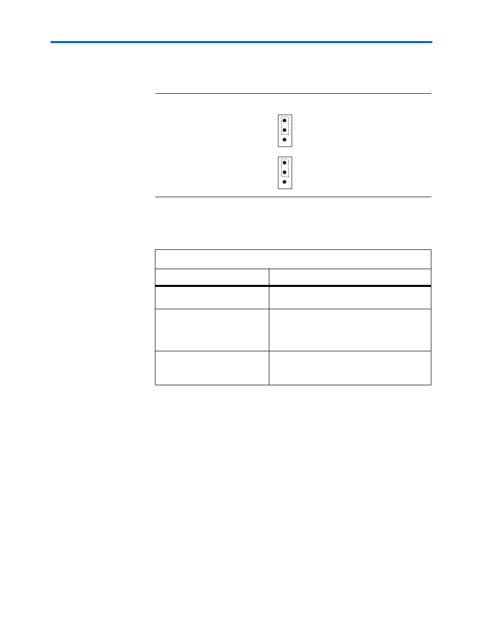
shows J18 and J19 with sample jumpers placed on pins 1 and
2. This setting selects the on-board clock oscillator as the input to U16.
Figure 2–23. J18 & J19 Pin-Outs
lists the setting on J18 and J19 that select desired input to be
input to U16
CLK SMA Connector (J17)
The CLK SMA connector (J17) provides an external clock input. It can be
selected to be the input to U16. J17 is shown in
An external clock source provides designers, while using a particular
design, the flexibility to alter the input frequency to verify F
MAX
tolerances.
On-Board/Custom Clock Oscillators Select Jumper (J18)
J18 selects the on-board clock oscillator (U20) or the custom clock
oscillator (J20) as the selected clock oscillator to be input to U16. See
Table 2–31. Selecting the Clock Input to U16
Clocking Option
Settings
On-board clock oscillator (U20)
●
On J18, place a jumper on pins 1 and 2.
●
On J19, place a jumper on pins 1 and 2.
Custom oscillator (J20)
●
Plug a custom half-can oscillator into the
J20 socket.
●
On J18, place a jumper on pins 2 and 3.
●
On J19, place a jumper on pins 1 and 2.
SMA connector (J17)
●
Use J17 (
CLK_SMA
) for external clock
input.
●
On J19, place a jumper on pins 2 and 3.
OSC
SMA
SMT OSC
SKT OSC
J19
1
3
J18
1
3