Altera Cyclone II DSP Development Board User Manual
Page 27
Advertising
Altera Corporation
Reference Manual
2–19
August 2006
Cyclone II DSP Development Board
Cyclone II DSP Development Board Components
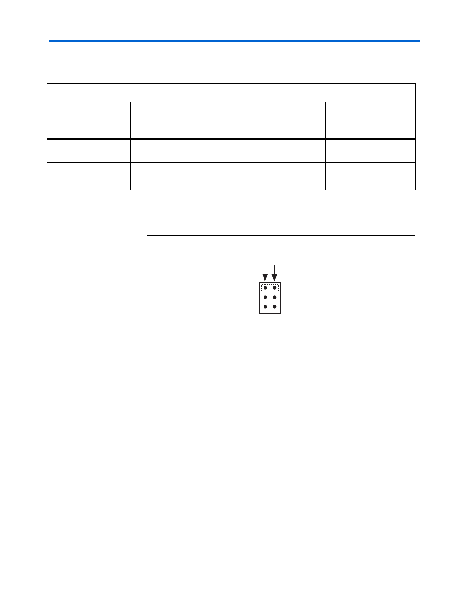
lists the J35 jumper settings used to select the D/A clock.
shows the J35 and J34 pin-outs listed in
. Pins 1 and
2 show an example jumper setting used to select the OSC clock.
Figure 2–8. J35 & J34 Pin Settings
Table 2–12. TI DAC904E D/A Converter (U25 & U30) Clock Source Settings
Clock Source
Board Reference
Schematic Signal Name
D/A Converter Clock
Select (J35 & J34)
Setting
OSC clock
OSC
CLK_OSC_DACA
(Channel A)
CLK_OSC_DACB
(Channel B)
Pins 1 and 2
FPGA clock
PLL
FPGA_TO_DAC_CLK
Pins 3 and 4
SMA clock (J26)
SMA
SMA_TO_DAC_CLK
Pins 5 and 6
J35 or J34
Pin 1
Pin 2
OSC
PLL
SMA
Advertising