A/d converter clocks, Figure 2–9 – Altera Cyclone II DSP Development Board User Manual
Page 31
Altera Corporation
Reference Manual
2–23
August 2006
Cyclone II DSP Development Board
Cyclone II DSP Development Board Components
Figure 2–9. J30 & J38 Pin Settings
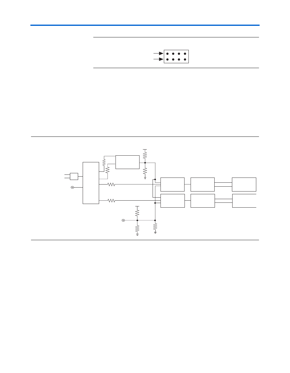
A/D Converter Clocks
shows the components involved in selecting the clock signal
to be sent to the TI ADS5520 A/D converter (U26 for channel A, U31 for
channel B). J37 (channel A) or J36 (channel B) selects the A/D clock from
the OSC clock, the FPGA clock, or the SMA clock (J27). The selected A/D
clock passes through a differential LVPECL buffer (U29 for channel A,
U28 for channel B), which provides the clock signal to the TI ADS5520.
Figure 2–10. TI ADS5520 A/D Converter Clocking Options
Refer to
“Clock Circuitry” on page 2–59
for information on clock source selection.
J30 & J38
Pin 1
Pin 2
ADC External Clock SMA (J27)
50
143
95.3
143
95.3
33
J37
ADC Clock
Select
U12
EP2C35
FPGA_TO_ADC_CLK
SMA_TO_ADC_CLK
CLK_OSC_ADCA
U29
ADC Clock
Buffer
U26
TI ADS5520
+
-
External Clock SMA (J17)
U16
Clock
Buffer
On-Board Clock (U20)
Custom Clock (J20)
J18
CLKIN_TOP
CLKIN_BOT
33
33
33
J36
ADC Clock
Select
CLK_OSC_ADCB
U28
ADC Clock
Buffer
U31
TI ADS5520
+
-