A/d converter clock buffer (u29 & u28), A/d converter (u26 & u31), Table 2–16 on – Altera Cyclone II DSP Development Board User Manual
Page 30
2–22
Reference Manual
Altera Corporation
Cyclone II DSP Development Board
August 2006
User Interfaces
A/D Converter Clock Buffer (U29 & U28)
U29 provides the selected A/D clock to U26 for channel A. U28 provides
the selected A/D clock to U31 for channel B. For more information, see
“A/D Converter (U26 & U31)” on page 2–22
A/D Converter (U26 & U31)
The Cyclone II DSP development board contains one TI ADS5520 12-bit
125 MSPS A/D converter. The device is designed for high speed and
high-performance applications.
The input to this A/D converter is transformer-coupled in order to create
a balanced input. To maximize performance, two transformers (T2, T3)
are used in series. The signal-to-noise ratio for the system is 70 dB for
input signals from 1 MHz to the Nyquist frequency of the converter. The
maximum differential input voltage to the converter is 2.2 V
PP
.
lists the A/D converter references.
The data output format from the A/D converter is selectable through J30
(channel A) or J38 (channel B).
lists the available data output
format options and how to set them.
shows the pin settings for
J30 and J38.
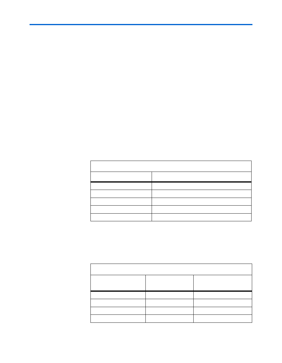
Table 2–15. A/D Converter Reference
Item
Description
Board reference
U26 (channel A) and U31 (channel B)
Part number
ADS5520
Device description
12-bit 125 MSPS A/D converter
Manufacturer
Texas Instruments
Manufacturer web site
www.ti.com
Table 2–16. TI ADS5520 A/D Converter (J26) Data Output Format Select
Jumper (J30 & J38)
Setting
Data Format
Clock Output Polarity
Pins 1 and 2
Two’s Complement
Data valid on falling edge
Pins 3 and 4
Straight Binary
Data valid on falling edge
Pins 5 and 6
Two’s Complement
Data valid on rising edge
Pins 7 and 8
Straight Binary
Data valid on rising edge