Ddr2 sdram dimm clocks – Altera Cyclone II DSP Development Board User Manual
Page 35
Altera Corporation
Reference Manual
2–27
August 2006
Cyclone II DSP Development Board
Cyclone II DSP Development Board Components
For information about the pin-outs between the Altera DDR2 Controller
MegaCore
®
function and the Cyclone II DSP development board, see
Appendix A, DDR2 SDRAM DIMM Connector Pin Out Table
lists the DDR2 SDRAM DIMM device reference.
DDR2 SDRAM DIMM Clocks
shows the interface to the DDR2 SRRAM DIMM and the
required clocking.
shows the use of the dedicated DDR2
SRRAM DIMM (J8) DQS pins to clock the byte lanes. All clock outputs
from the Cyclone II DSP development board use ALTDDIO output
registers that can be sourced from any I/O pin. The maximum speed for
this interface is 167 MHz.
1
The J8 connector is Class I terminated.
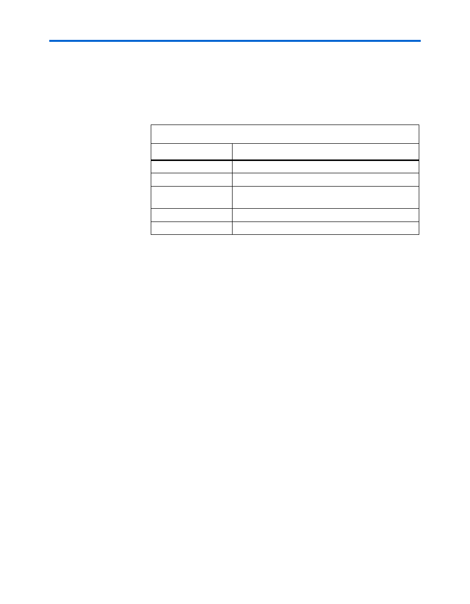
Table 2–20. DDR2 SDRAM DIMM Device Reference
Item
Description
Board reference
J8
Part number
MT8HTF3264AY-40E
Device description
256 Mbyte, 32 Mbyte x 64, 167 MHz, 1.8 V, 240-pin,
non-ECC, unbuffered DDR2 SDRAM DIMM
Manufacturer
Micron Technology
Manufacturer web site
www.micron.com