Dimm_sync_clk sma connector (j11), Note (1) – Altera Cyclone II DSP Development Board User Manual
Page 44
2–36
Reference Manual
Altera Corporation
Cyclone II DSP Development Board
August 2006
Memory Components
DIMM_SYNC_CLK SMA Connector (J11)
A special feedback clock signal called DIMM_SYNC_CLK is included on
the board with an SMA(J11) at the end of the trace near its termination
point resistor. This signal has two purposes:
■
You can use this signal as a test point SMA for eye diagrams of DDR2
signals using AC-coupled SMA connections to an oscilloscope.
■
You can use this signal as a board-level round trip delay estimator as
an optimal method in resynchronizing DDR2 DIMM read captures
with the internal clock (output from the PLL in
). The
length of DIMM_SYNC _CLK is the same as the output clocks
(.e.g.DIMM_CK_PO) and the return clocks (e.g.DIMM_DQSO).
83
92
102
104
113
126
135
147
156
165
203
212
224
Notes to
(1)
Blank cells indicate no connection.
(2)
In the Cyclone II Signal Name column, some of the names are different than the
DIMM (J8) Signal Name due to the use of series resistors.
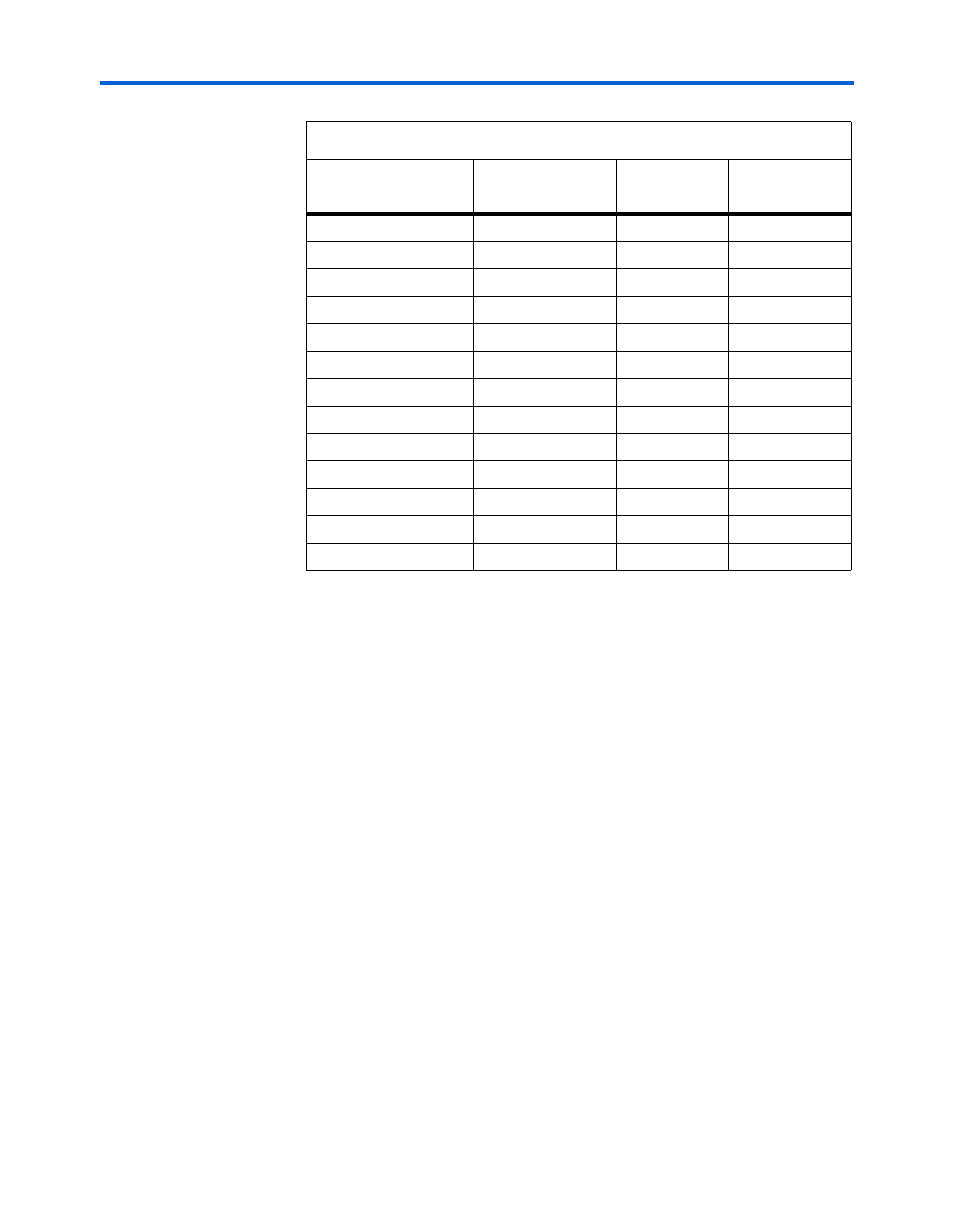
Table 2–21. DDR2 SDRAM DIMM Pin-Outs (Part 8 of 8)
Note (1)
Cyclone II (U12)
Signal Name
(2)
DIMM (J8) Signal
Name
(2)
DIMM (J8) Pin
Number
Cyclone II (U12)
Pin Number