Appendix b. ssram pin-out table, Introduction, Appendix b, ssram – Altera Cyclone II DSP Development Board User Manual
Page 83: Pin-out table, Appendix b, Ssram pin-out table
Altera Corporation
Reference Manual
B–1
August 2006
Preliminary
Appendix B. SSRAM
Pin-Out Table
Introduction
Because the SSRAM component and the TI EVM board’s EMIF interface
are bussed, there is a mapping between the signal names. The printed
circuit board (PCB) signal names connecting the Cyclone™ II
EP2C70F672 FPGA designates the EVM naming conventions. Even
though both the SSRAM and TI-EVM have address and data busses they
do not map directly (for example, EVM_D0 connects to SRAM_D15).
lists the mapping. Use this table to create designs that directly
interface to the SSRAM.
The Cyclone II signal name corresponds to the net name at the
EP2C70F672 FPGA. The SRAM signal name is the net name at the
SSRAM.
1
There is a 22-
Ω series resistor between the EP2C70F672 pins and
the SSRAM device pins. The SSRAM pin name corresponds to
the name assigned to the pin in the SSRAM data sheet.
f
See the Cypress CY7C1360B 9-Mbit (256K x 36/512K x 18) Pipelined SRAM
on the Cypress Web site at www.cypress.com.
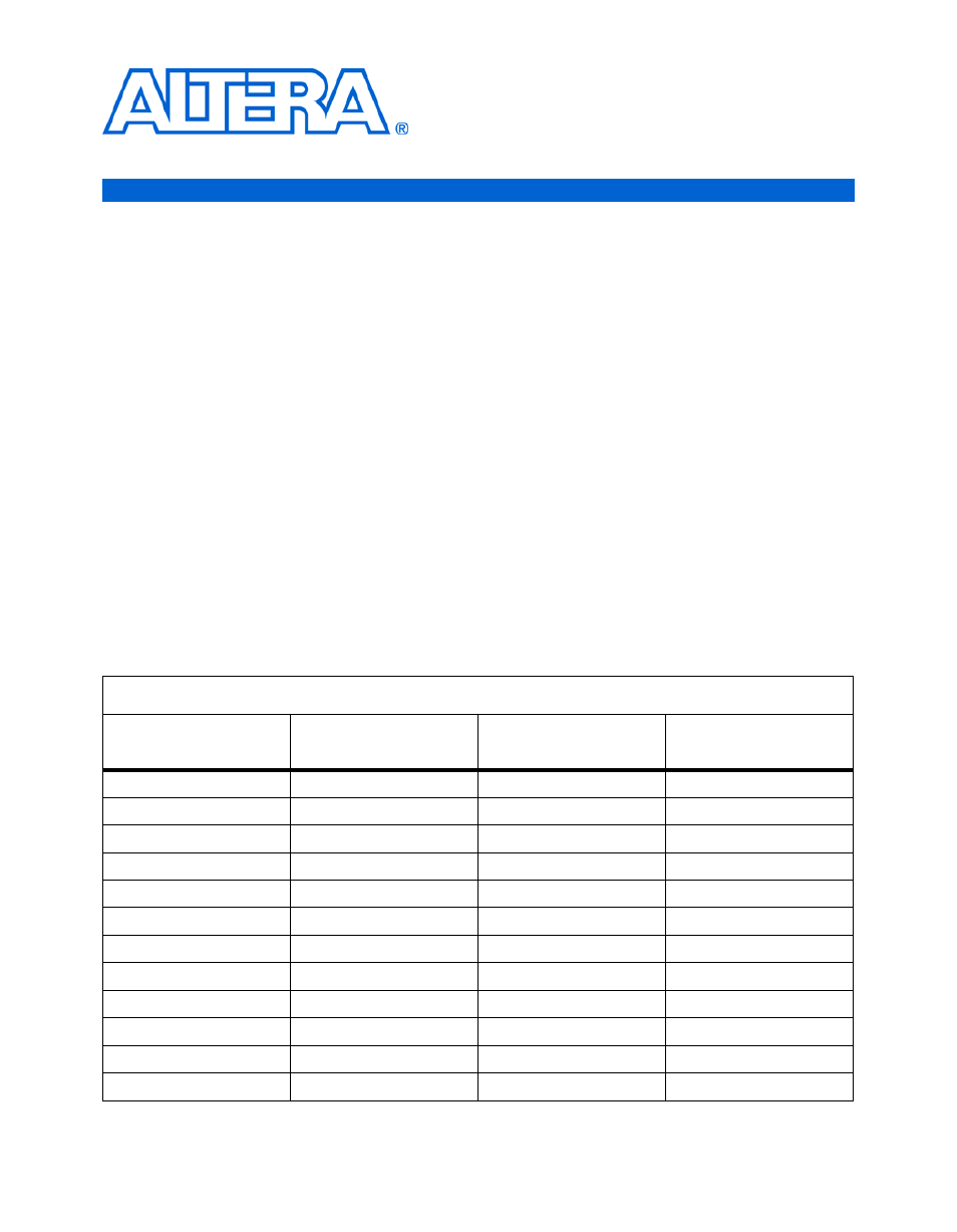
Table B–1. Cyclone II to SSRAM Device Signal Changes (Part 1 of 3)
Cyclone II (U12) Signal
Name
SSRAM (U22) Signal
Name
SSRAM (U22) Pin
Cyclone II (U12) Pin
Name
EVM_A2
SRAM_A2
82
E25
EVM_A3
SRAM_A3
33
L24
EVM_A4
SRAM_A4
81
E26
EVM_A5
SRAM_A5
35
L25
EVM_A6
SRAM_A1
36
E24
EVM_A7
SRAM_A0
37
K26
EVM_A8
SRAM_A18
38
E23
EVM_A9
SRAM_A19
39
K25
EVM_A10
SRAM_A6
100
D26
EVM_A11
SRAM_A11
43
J26
EVM_A12
SRAM_A12
44
D25
EVM_A13
SRAM_A13
45
K24