Altera Cyclone II DSP Development Board User Manual
Page 15
Altera Corporation
Reference Manual
2–7
August 2006
Cyclone II DSP Development Board
Cyclone II DSP Development Board Components
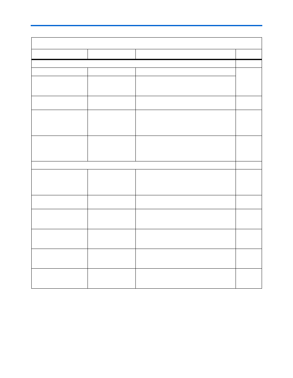
Status LEDs & Reset/Power Switches
D1
Power LED
Indicates when power is present.
D10
Status LED
Indicates successful configuration of the
Cyclone II DSP development board
(
CONFIG_DONEn
is asserted).
SW1
Power switch
Power switch that is used to apply power to the
on-board power regulators.
SW6
User-defined reset
push-button
USER RESET is user-defined
momentary-contact push-button used to reset
and initialize a user design on the Cyclone II
DSP development board.
SW7
System reset
push-button
SYS RESET is a momentary-contact push-
button used to reset the hardware and configure
the Cyclone II DSP development board with the
design stored in the EPCS64 selected by J29.
Clocks
J20
Socket for connecting
custom clock
oscillator
Socket on top of U20 where a half-can clock
oscillator can be installed. It is referred to as the
custom clock oscillator. It can be an input to
U16.
U16
Clock buffer
U16 is the clock buffer for the five clocks on the
Cyclone II DSP development board.
U20
On-board clock
oscillator
The on-board clock oscillator is the ECS, Inc.
ECS-3953M-1000-BN-TR 100 MHz surface
mount oscillator. It can be an input to U16.
U27
D/A converter clock
buffer
U27 uses the DAC_A clock selected by J35 and
inputs it to U25, and uses the DAC_B clock
selected by J34 and inputs it to U30.
U29
A/D converter
differential LVPECL
buffer
U29 uses the ADC_A clock selected by J37 and
inputs it to U26.
U28
A/D converter
differential LVPECL
buffer
U28 uses the ADC_B clock selected by J36 and
inputs it to U31.
Table 2–1. Cyclone II DSP Development Board Components & Interfaces (Part 4 of 5)
Board Reference
Name
Description
Page