Memory components, Ddr2 sdram dimm (j8) – Altera Cyclone II DSP Development Board User Manual
Page 34
2–26
Reference Manual
Altera Corporation
Cyclone II DSP Development Board
August 2006
Memory Components
Memory
Components
This section describes the memory components on the Cyclone II DSP
development board.
DDR2 SDRAM DIMM (J8)
The Cyclone II DSP development board contains a single slot connector
(J8) for a 240-pin DDR2 DIMM module. It has a 72-bit data interface with
a full 16-bit address, a 3-bank interface, and supports single and
double-sided passive or registered design DIMMs.
The DDR2 SDRAM DIMM is a 256 Mbyte unbuffered non-ECC device in
a x64 configuration.
1
Cyclone II DSP development board uses x64 configuration. The
maximum transfer rate of this DIMM is 333 Mbps. The total is
333 Mbps × 8 = 2,664 Mbps.
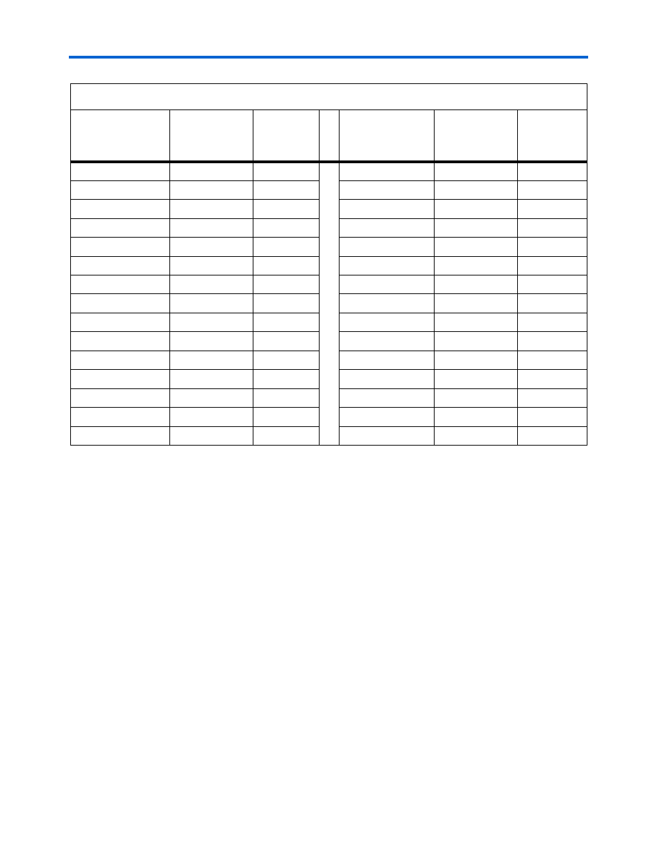
Table 2–19. TI ADS5520 A/D Converter and EP2C70F672 Pin-Outs
A/D Converter
(U31) Pin Name
A/D Converter
(U31) Pin
Number
Cyclone II
(U12) Pin
Number
A/D Converter
(U31) Pin Name
A/D Converter
(U31) Pin
Number
Cyclone II
(U12) Pin
Number
ADC_B_CLK_N
11
ADC_B_D5
52
B20
ADC_B_CLK_P
10
ADC_B_D6
53
A20
ADC_B_CM
17
ADC_B_D7
54
B21
ADC_B_DCLK
43
C13
ADC_B_D8
55
F18
ADC_B_DFS
40
ADC_B_D9
56
G18
ADC_B_INM
20
ADC_B_D10
60
E18
ADC_B_INP
19
ADC_B_D11
61
F20
ADC_B_IREF
31
ADC_B_D12
62
D21
ADC_B_OE
41
R2
ADC_B_D13
63
D20
ADC_B_OVR
64
A6
ADC_B_REFM
30
ADC_B_D0
44
F17
ADC_B_REFP
29
ADC_B_D1
45
D17
ADC_B_SEN
4
D19
ADC_B_D2
46
D18
ADC_RESET
35
T24
ADC_B_D3
47
C19
ADC_SCLK
2
AD24
ADC_B_D4
51
B19
ADC_SDATA
3
Y1
Note to
(1)
Blank cells indicate no connection.