Introduction – Altera Cyclone II DSP Development Board User Manual
Page 79
Altera Corporation
Reference Manual
A–1
August 2006
Preliminary
Appendix A. DDR2 SDRAM
DIMM Connector Pin Out Table
Introduction
The printed circuit board (PCB) layout for the DDR2 SDRAM DIMM
interface to the Cyclone™ II EP2C70 FPGA was optimized for a reduced
layer count, reduced via count, and improved signal integrity. This
required swapping names from the pin locations created by the DDR2
MegaCore
®
function’s placement and pin-out tool command language
(Tcl) script. These swaps only occurred within each octal byte lane (for
example, DQ0-DQ7). The result is that, for example, a DDR2 SDRAM
DIMM FPGA design in the Quartus
®
II software will have an I/O called
DIMM_DQ0 (data bit 0) but the corresponding net name on the schematic
that this logical pin is connected to is called DIMM_DQ7 (data bit 7).
Conversely, the DIMM_DQ7 bit is driven to net named DIMM_DQ0. This
swapping list is provided in
.
Use the DDR2 MegaCore function’s default pinout script location for the
EP2C70F672 interface width and do not re-assign the pins to match the
Cyclone II DSP development board’s signal names as DQ data pins. Use
if you need to track a particular signal to its destination for
eye-diagrams or for general debugging purposes.
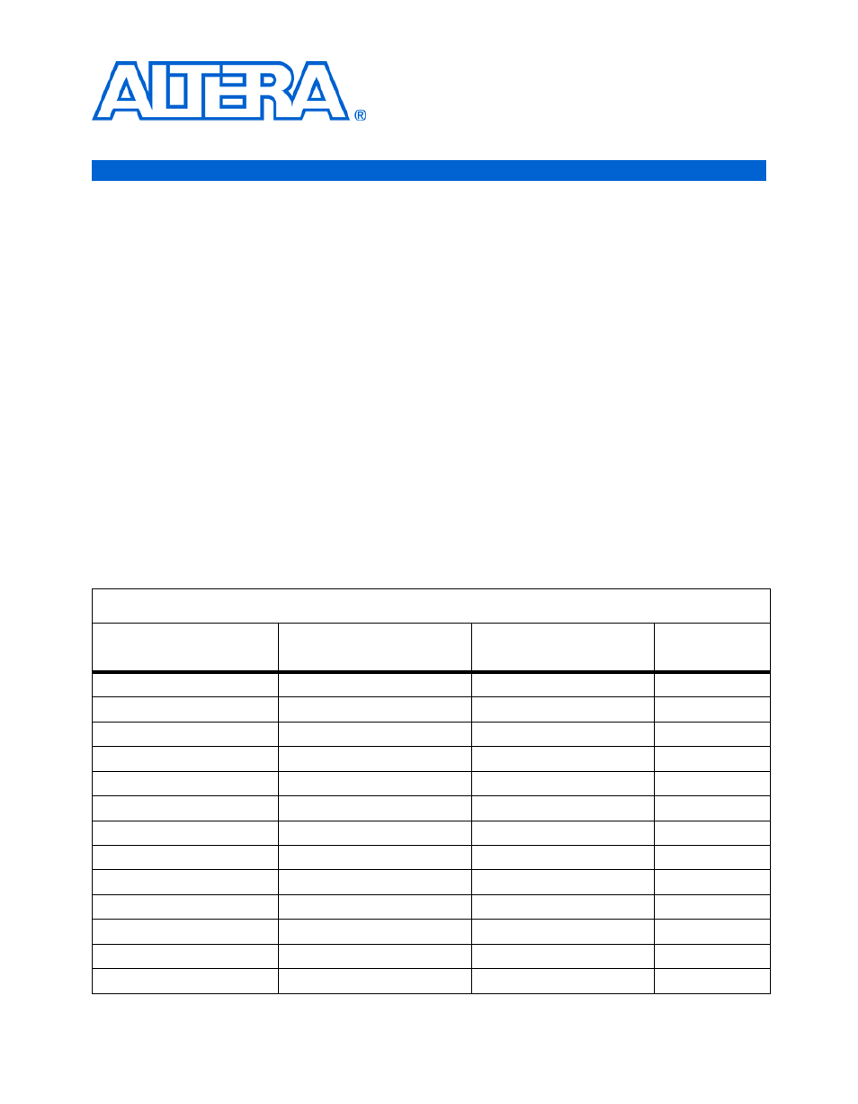
Table A–1. Cyclone II EP2C70F672 DSP Development Board to DIMM Pin Changes (Part 1 of 4)
Signal Name
Original DDR2 Core Location
EP2C70F672 Board
Location
Different
(Yes/No)
DIMM_DQ0
AD16
AA16
Yes
DIMM_DQ1
AF17
AC17
Yes
DIMM_DQ2
AE17
AE17
No
DIMM_DQ3
AC17
AF17
Yes
DIMM_DQ4
AD17
Y16
Yes
DIMM_DQ5
AA16
AD17
Yes
DIMM_DQ6
Y16
AF18
Yes
DIMM_DQ7
AF18
AD16
Yes
DIMM_DQ8
AD12
Y15
Yes
DIMM_DQ9
AE12
AA15
Yes
DIMM_DQ10
AC14
AC14
No
DIMM_DQ11
AA13
AD12
Yes
DIMM_DQ12
Y13
Y13
No