Command and status registers (csrs), Command and status registers (csrs) –15 – Altera RapidIO MegaCore Function User Manual
Page 147
Chapter 6: Software Interface
6–15
Transport and Logical Layer Registers
August 2014
Altera Corporation
RapidIO MegaCore Function
User Guide
Command and Status Registers (CSRs)
through
describe the command and status registers.
ATM_TEST_SWP
[8]
RO
Processing element can support an ATOMIC test-and-swap
operation
1'b0
ATM_INC
[7]
RO
Processing element can support an ATOMIC increment operation 1'b0
ATM_DEC
[6]
RO
Processing element can support an ATOMIC decrement operation 1'b0
ATM_SET
[5]
RO
Processing element can support an ATOMIC set operation
1'b0
ATM_CLEAR
[4]
RO
Processing element can support an ATOMIC clear operation
1'b0
ATM_SWAP
[3]
RO
Processing element can support an ATOMIC swap operation
1'b0
PORT_WRITE
[2]
RO
Processing element can support a port-write operation
Implementation
Defined
[1:0]
RO
Reserved for this implementation
2'b00
Notes to
:
(1) If none of the Logical layers supported by the RapidIO MegaCore is selected, the corresponding bits in the Source and Destination Operations
CAR are forced to zero. These bits cannot be set to one, even if the corresponding operations are supported by user logic attached to the
Avalon-ST pass-through interface.
(2) The default value is 1'b1 if the Avalon-MM Master is selected as an Input/Output Logical layer interface in the RapidIO parameter editor. If the
Avalon-MM Master is not selected, the value is 1'b0.
(3) The default value is set in the RapidIO parameter editor.
(4) The default value is 1'b1 if Doorbell Rx enable is turned on in the RapidIO parameter editor. If Doorbell Rx enable is turned off, the value is
1'b0
.
(5) The default value element is 1'b1 if Port Write Rx enable is turned on in the RapidIO parameter editor. If Port Write Rx enable is turned off,
the value is 1'b0.
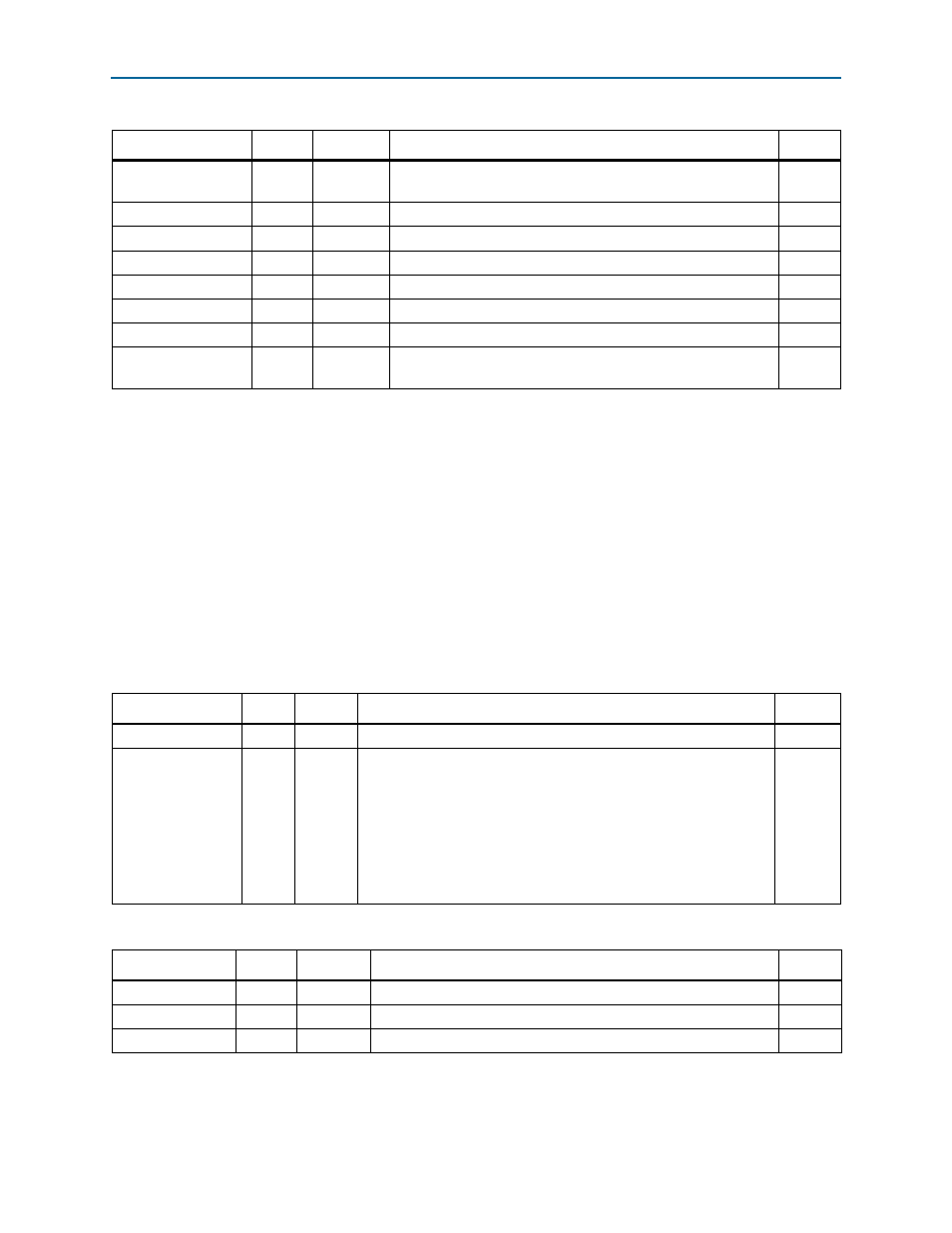
Table 6–19. Destination Operations CAR—Offset: 0x1C
(1)
(Part 2 of 2)
Field
Bits
Access
Comment
Default
Table 6–20. Processing Element Logical Layer Control CSR—Offset: 0x4C
Field
Bits
Access
Function
Default
RSRV
[31:3]
RO
Reserved
29'h0
EXT_ADDR_CTRL
[2:0]
RO
Controls the number of address bits generated by the Processing
element as a source and processed by the Processing element as the
target of an operation.
'b100 – Processing element supports 66 bit addresses
'b010 – Processing element supports 50 bit addresses
'b001 – Processing element supports 34 bit addresses
All other encodings reserved
3'b001
Table 6–21. Local Configuration Space Base Address 0 CSR—Offset: 0x58
Field
Bits
Access
Function
Default
RSRV
[31]
RO
Reserved
1'b0
LCSBA
[30:15]
RO
Reserved for a 34-bit local physical address
16'h0
LCSBA
[14:0]
RO
Reserved for a 34-bit local physical address
15'h0