Stratix gx hssdc2 xcvr functional description – Altera High-Speed Development Kit, Stratix GX Edition User Manual
Page 115
Altera Corporation
Quartus II Version 3.0
7–33
Diagnostic Test Details
Standard Tests
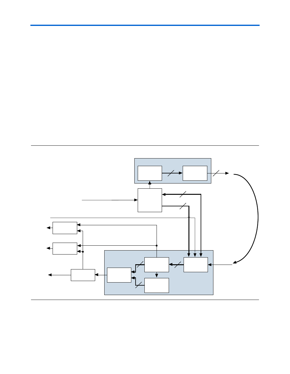
word feature, the byte alignment of the received data may be incorrect.
To adjust it, the data is sent through a byte swap block based on
synchronization data from the GXB megafunction. The data is then
passed to a pattern detection block to find the start of data in the PRBS
(the first word of the PRBS sequence) data stream. When this pattern is
found, the data valid signal is asserted, which triggers an expected value
PRBS generator to start. The two data streams are sent to a comparator to
generate a match signal on a per channel basis. If the data streams match,
the match LED illuminates on a per channel basis. If the match signal goes
low while the data valid signal is high, the error flag is set and the error
counter is incremented. Pressing the reset pushbutton resets the system
state, error flag, and error count.
Stratix GX HSSDC2 XCVR Functional Description
Figure 7–16 shows the Stratix GX HSSDC2 XCVR logic diagram.
Figure 7–16. Stratix GX HSSDC2 XCVR Logic Diagram
The GXB megafunction transmit PLL generates the system clock using
the 156.25-MHz crystal as the reference. The PLL generates a 156.25-MHz
clock to clock all of the data generation logic.
Loopback with 2
HSSDC2 Cables
PRBS
Generator
ALT GXB
TX
Transmit Channel (x4)
20
1
Start/Stop
Synchronization
Detect/Control
4
8
Receive
Equalization
Dipswitch 1,0
ALTGXB
RX
Comparator
Receive Channel (x4)
20
20
22
Match
Register
Data Valid
Error
Register
Error
Counter
Data Valid
PRBS
Generator
7-Segment
Display
Error LED
Match LED
Pattern Detect/
Byte Swap