8 pciexpress interface, Figure 9-5, Pciexpress subsystem block diagram – Artesyn ARTM-831X Installation and Use (June 2014) User Manual
Page 167
TSI FPGA
ARTM-831X Installation and Use (6806800M76E)
167
9.4.8
PCIexpress Interface
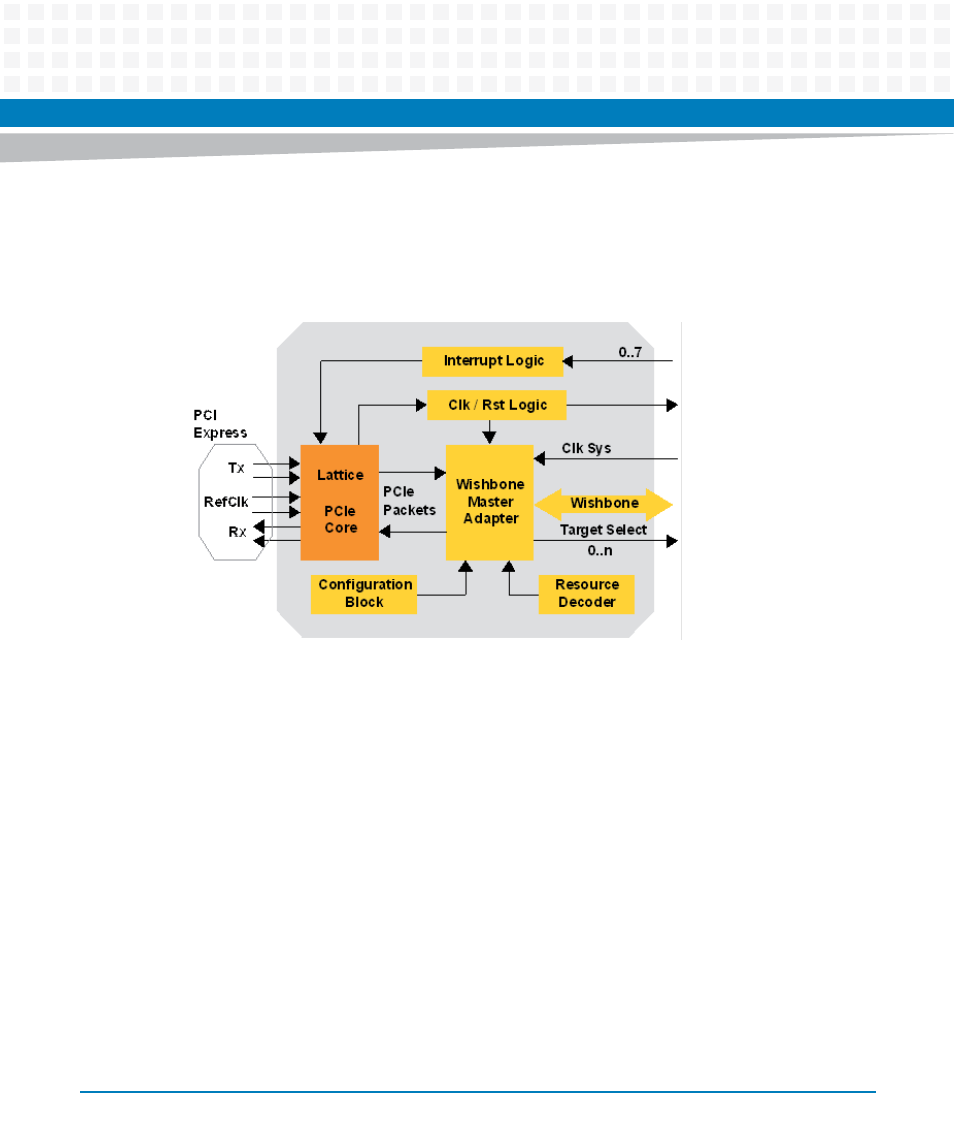
A block diagram of the PCIexpress subsystem can be seen in Figure 4.
The clock/reset logic receives a 125 MHz clock from the Lattice PCIexpress core. This is in turn
derived from the 250 MHz symbol clock on the PCIexpress interface. Additional signals from
the PCIexpress core, such as link down, are monitored to determine when a warm or hot reset
must be generated.
The configuration block is an output only block. It uses the configuration file for the Lattice
PCIexpress core and forwards the configuration settings to the Wishbone Master Adapter. This
ensures that there is a single point of change for the core configuration. Settings such as
infinite/non-infinite credits, use of PCI base address registers etc. are passed to the Wishbone
Master Adapter.
The interrupt logic block receives up to eight interrupts from the user logic. The user interrupts
are forwarded to the legacy-interrupt or message-signalled interrupt inputs of the Lattice
PCIexpress core, depending on whether legacy interrupts or message-signalled interrupts
(MSI) are enabled by the system software.
Figure 9-5
PCIexpress Subsystem Block Diagram