Tsi fpga, 3 scratchpad register, 4 test mode control register – Artesyn ARTM-831X Installation and Use (June 2014) User Manual
Page 263
TSI FPGA
ARTM-831X Installation and Use (6806800M76E)
263
9.5.2.12.3 ScratchPad Register
Address:
0x1508, ScratchPadReg
Width: 32 bit
Register memory without any control or status function
9.5.2.12.4 Test Mode Control Register
Address:
0x150C, TestModeCtrlReg
Width: 8 bit
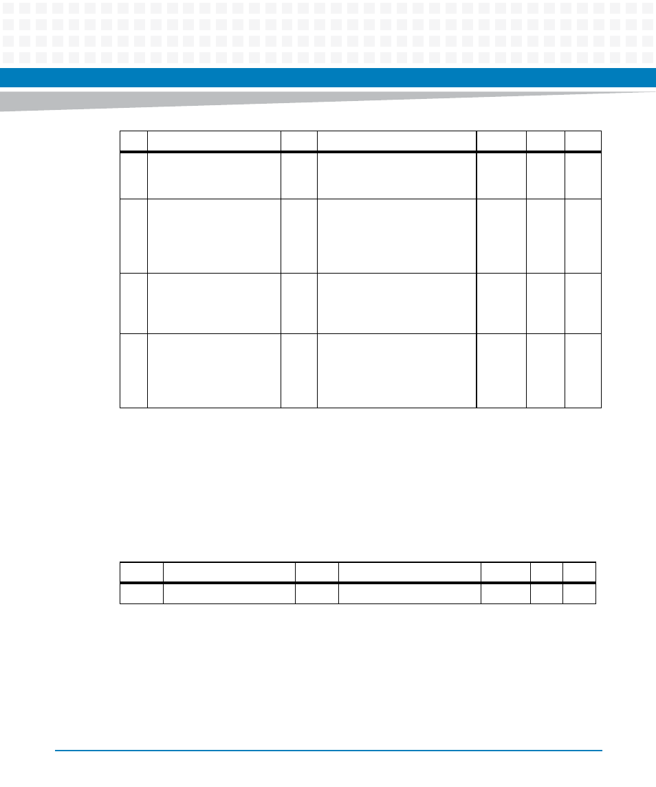
3
NoTdmEsfSyncForce
RW
0b1: NoTdmEsfSyncForce, force
no main extended superframe
166.66Hz sync pulse indicator
0b0
X
X
2
NoMainTdmFrameSyncFo
rce
RW
0b1:
NoMainTdmFrameSyncForce,
force no main frame sync 8kHz
pulse from TDM system clock
generator indicator
0b0
X
X
1
NoMainClkPllLock77Forc
e
RW
0b1: NoMainClkPllLock77Force,
force main clock PLL 77.76 MHz
not locked to TDM system clock
indicator
0b0
X
X
0
NoMainClkPllLock131For
ce
RW
0b1:
NoMainClkPllLock131Force,
force main clock PLL
131.072MHz not locked to TDM
system clock indicator
0b0
X
X
Bit
Acronym
Type
Description
Default
Pwr
Soft
Bit
Acronym
Type
Description
Default
Pwr
Soft
31...0
ScratchPadData
RW
Scratch Pad Data
0b0
X
X