Altera DDR Timing Wizard User Manual
Page 36
2–24
Altera Corporation
DDR Timing Wizard User Guide
November 2007
Entering and Editing Inputs to the DTW
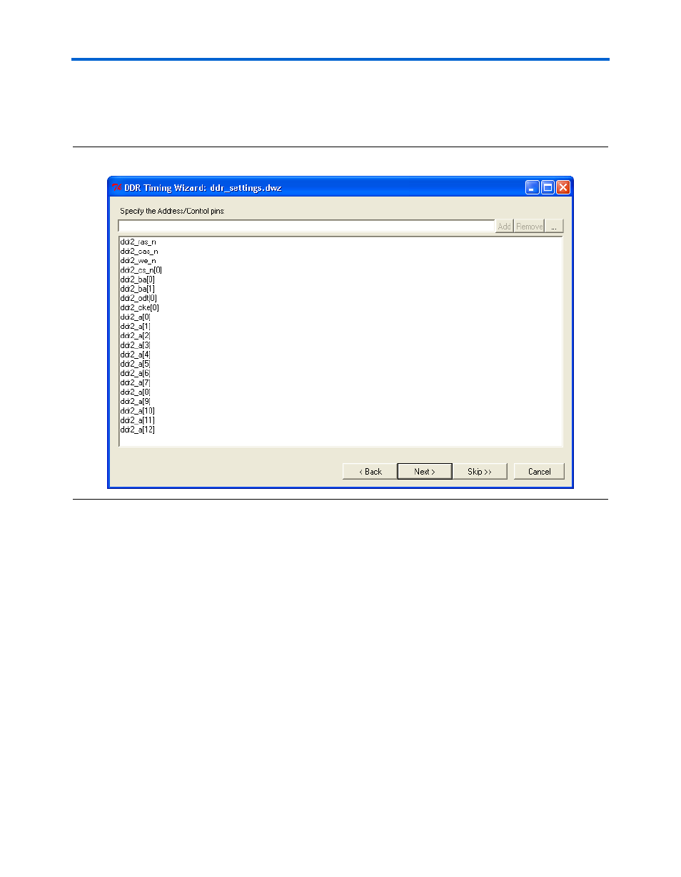
10. Identify the address and control pins. The sample list of the address
and control pins for a DDR2 SDRAM interface is shown in
Figure 2–18. Sample Page of Filled Address and Control Pins Page
Click Next.
11. When the DTW has all of the pin connectivity information, set up
the design resynchronization clocking scheme as shown in
, which uses the legacy controller MegaWizard default
name clock selection.
1
The clock input frequency, multiplication, division, phase
shifts, and clock cycle selection differ from design to design.
1
The resynchronization page selection for QDRII+/QDRII
SRAM and RLDRAM II interfaces do not have any clock
cycle or phase shift selections. You can also indicate that
you are using a FIFO for resynchronization in these
interfaces.