Altera DDR Timing Wizard User Manual
Page 82
3–22
Altera Corporation
DDR Timing Wizard User Guide
November 2007
Timing Closure Process
1
Note that if only 1 or 2 pins fail timing, you can adjust the
appropriate delay chain settings in the Assignment Editor,
instead of changing PLL phase shifts.
To decide whether it is safe to change the phase shift of a clock, check
whether the clock is being used anywhere else in the design. You must
never change the phase shift of the system clock (pllclk[0]) or the
write clock (pllclk[1]) which default to 0° and -90°, respectively, in the
DDR2/DDR SDRAM and RLDRAM II memory interface. In
QDRII+/QDRII SRAM interfaces, the system clock is still at 0°, but the
write clock is at 90°. The system clock is used throughout the PHY and
controller, so changing this clock changes the timing relationship of the
whole interface. The write clock needs to have 90° phase-shift
relationship with the system clock unless write capture does not meet
timing requirements.
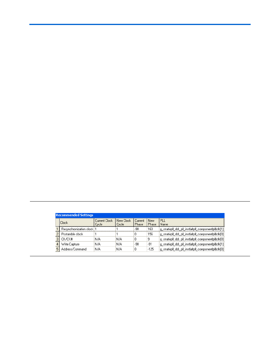
shows an example of the Recommended Settings panel for a
1-PLL mode. Note that the panel does not show the fedback clock or
system postamble clock as these clocks are not used in the 1-PLL
implementation. In this example, the postamble, the CK/CK#, and
address/command clocks share the same PLL output clock (output
pllclk[0]
which is also the system clock), while the resynchronization
and the write capture clocks share PLL output pllclk[1], the DQ write
clock that is -90° phase-shifted from the system clock. This means that if
you change these clocks, multiple paths are affected, so you must be
careful before changing any phase shift.
Figure 3–11. Example for the Recommended Settings Panel for 1-PLL Memory Interface
For the example shown in
, instead of changing pllclk[1],
you should use a different PLL output for the resynchronization clock.
Similarly, instead of changing pllclk[0], you can use two different
PLL output clocks: one for the postamble clock and one for the
address/command clock. For this particular example, you can also share
the same PLL output clock for resynchronization and postamble clocks,
since they are 7° (163° - 156°) apart. However, you may need to change
the resynchronization clock cycle to 2 to let data propagate from the IOEs
gated by the postamble clock to the resynchronization registers.