Altera DDR Timing Wizard User Manual
Page 71
Altera Corporation
3–11
November 2007
DDR Timing Wizard User Guide
Using the dtw_timing_analysis.tcl Script
When you must change a PLL output phase shift that will affect
another path adversely, create another PLL output tap instead. This
requires manual RTL changes and editing the PLL clock usage.
shows the path recommended by the script for the
different memory interfaces.
Typically, the write timing paths use a variation of the system or the
write clock.
shows some variations of the available clocks
that the Altera DDR2 SDRAM Controller MegaCore function may
use.
to achieve 0°, 90°, 180°, or
270° in your design. However, if the phase shift required is not one
of the four options, you may need to add a dedicated PLL output and
change the clock connections for these paths to achieve the best
margin. For interfaces above 200 MHz, Altera recommends to always
use a dedicated PLL output.
Dedicated
postamble clock
Classic
Timing
Analyzer
*:g_stratixpll_ddr_fedbackpll_inst|altpll:altpll_component|_clk1
TimeQuest
Timing
Analyzer
*g_stratixpll_ddr_fedback_pll_inst|altpll_component|pllclk[1]
Note to
:
(1)
System clock and write clock defaults to 0
°
and -90
°
phase shift, respectively, in DDR2/DDR SDRAM and RLDRAM II
memory interfaces. In QDRII+/QDRII SRAM interfaces, the system clock is 0
°
, but the write clock is at 90
°
. You must not
change the phase shift of these clocks, as it will affect the whole system.
Table 3–3. Default Clock Names and Usage in Altera DDR2 SDRAM Controller MegaCore Function
Note (1)
(Part 2
of 2)
Clock Usage
Timing
Analyzer
Clock Name
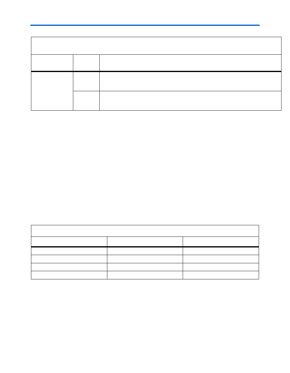
Table 3–4. Available Phase Shifts without Extra Dedicated PLL Outputs
Clock Usage
Variation
Phase Shift Achieved
System clock
Rising edge
0°
System clock
Falling edge
180°
Write clock
Rising edge
–90° or 270°
Write clock
Falling edge
90°