Timing closure process, Timing closure process –12 – Altera DDR Timing Wizard User Manual
Page 72
3–12
Altera Corporation
DDR Timing Wizard User Guide
November 2007
Timing Closure Process
■
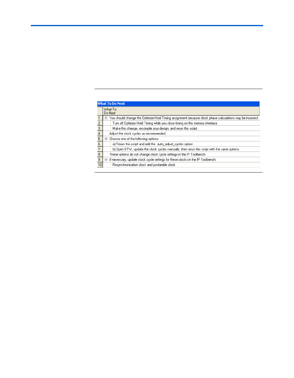
What To Do Next
This panel shows how to proceed in the design. If clock cycles need
changing, this panel details the necessary steps required before
moving on to fixing the phase shifts.
shows an example of the What To Do Next panel.
Figure 3–5. What To Do Next Panel
Remember to check the PLL output counter for each clock before
changing any phase shift. You should not change PLL output clocks
c0
(system clock) and c1 (write clock) as changing phase shift for
these clock will affect the memory controllers. Furthermore, PLL
output clock c0 may change the timing for the entire system since it
can be used as a system clock for the entire design. Instead, find out
if you can use a different PLL clock output instead to meet timing on
that particular path.
Timing Closure
Process
This section describes different situations that you may encounter in your
timing closure process. Most of the sub-sections below fall in the Adjust
Constraints
step of the memory interfaces design flow.
shows the timing closure process. You need to resynthesize
the design if you make any changes in the RTL files or MegaWizard GUI
to ensure that DTW is able to import the new settings. You can do so
manually or use the –import or –import_and_compile switch in the
dtw_timing_analysis.tcl
script.