Altera DDR Timing Wizard User Manual
Page 39
Advertising
Altera Corporation
2–27
November 2007
DDR Timing Wizard User Guide
Getting Started
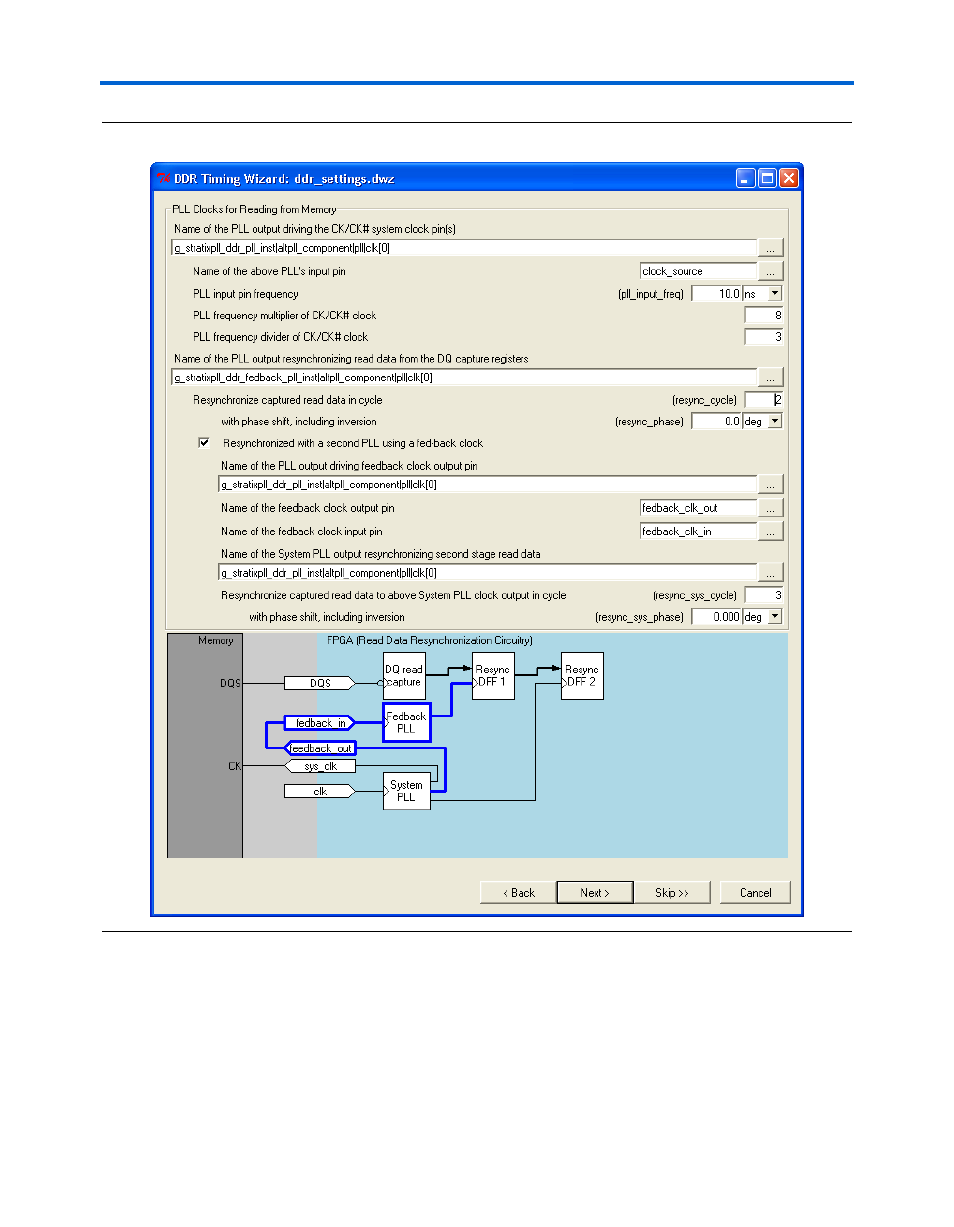
Figure 2–20. Fedback Resynchronization Path (Highlighted)
The first field of this page asks for the name of the PLL output
generating the CK/CK# system clock pins. Typically, this clock is the
system clock, which also drives the controller. However, if you are
using the dedicated clock output pins without the DDIO circuitry as
required in HardCopy II devices, you may need a separate PLL
output to ensure that t
DQSS
is met at both fast and slow timing
models.
Advertising