Figure 2–25, Show, Howe – Altera DDR Timing Wizard User Manual
Page 48
2–36
Altera Corporation
DDR Timing Wizard User Guide
November 2007
Entering and Editing Inputs to the DTW
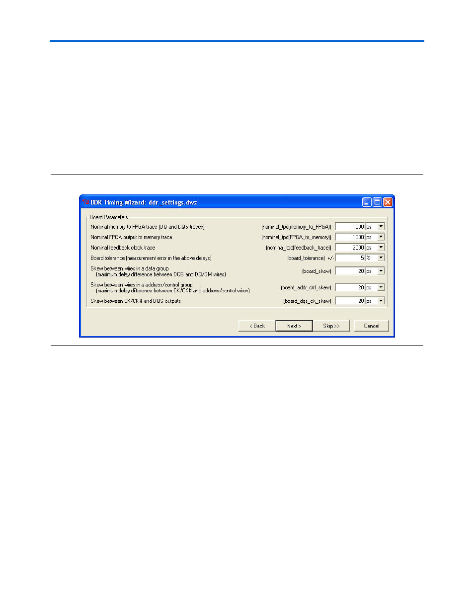
●
Skew between wires in an address/control group (maximum
delay difference between CK/CK# and address/control wires)
Maximum difference of BA, A, RAS#, CAS#, WE#, CS#, CKE,
and ODT board traces relative to CK/CK# board trace.
●
Skew between CK/CK# and DQS outputs
Maximum difference of CK/CK# board traces relative to
DQS/DQS# board traces.
Figure 2–25. Board Information Page with Default Legacy Controller MegaWizard Values
Click Next.
15. The next two pages, which are also the last two pages of the DTW,
are dependent on whether you are using TimeQuest or Classic
Timing Analyzer names. The second-to-last page shows the FPGA
parameters used for the interface, while the last page shows a
summary of the assignment as well as the location of the files that
contain the assignment.
show the FPGA parameter page of the
DTW when you are using TimeQuest or Classic Timing Analyzer
names, respectively. Both figures show a clock uncertainty section
with an option to use explicit clock uncertainties for HardCopy II
devices.