Altera JESD204B IP User Manual
Page 152
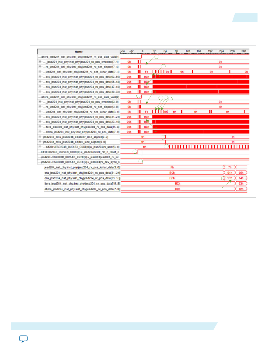
Figure 7-1: JESD204B Link Initialization
This is a SignalTap II image during the JESD204B link initialization. The JESD204B link has two
transceiver channels (L = 2).
f
b
a
j
k
e
c
d
d
g h i
c
f
start of 1st ILAS multi-frame
Description of the timing diagram:
a. The JESD204B link is out of reset.
b. The RX CDR is locked and PCS outputs valid characters to link layer.
c. No running disparity error and 8b/10b block within PCS successfully decodes the incoming
characters.
d. The ADC transmits /K/ character or BC hexadecimal number to the FPGA, which starts the CGS
phase.
e. Upon receiving 4 consecutive /K/ characters, the link layer deasserts the
rx_dev_sync_n
signal.
f. The JESD204B link transition from CGS to ILAS phase when ADC transmit /R/ or 1C hexadecimal
after /K/ character.
g. Start of 2
nd
multi-frame in ILAS phase. 2
nd
multi-frame contains the JESD204B link configuration
data.
h. Start of 3
rd
multi-frame.
i. Start of 4
th
multi-frame.
j. Device lanes alignment is achieved. In this example, there is only one device, the
dev_lane_aligned
connects to
alldev_lane_aligned
and both signals are asserted together.
k. Start of user data phase where user data is streamed through the JESD204B link
UG-01142
2015.05.04
Debugging JESD204B Link Using SignalTap II and System Console
7-5
JESD204B IP Core Debug Guidelines
Altera Corporation