Relationship between frame clock and link clock, Data bit and content mapping scheme – Altera JESD204B IP User Manual
Page 90
do not have this capability in the transport layer. If you needs to change any of these parameters, you
must recompile the system.
You are advised to connect the power down channels to higher indexes and connect used channel at lower
lanes. Otherwise, you have to reroute the physical-used channels to lower lanes externally when
connecting the IP core to the transport layer. For example, when L = 4 and csr_l = 8'd1 (which means two
lanes out of four lanes are active), with lane 1 and lane 3 being powered down, connection from the MAC
to the transport layer for lane 0 remains. However, lane 1 is powered down while lane 2 is not powered
down. Thus, lane 2 output from the MAC should be rerouted to lane 1 data input of the transport layer.
The data port for those power-down channels will be tied off within the transport layer.
The 16-bit N' data for F = 1 is formed through the data from 2 lanes. Thus, F = 1 is not supported for odd
number of lanes, for example, when LMF = 128. In this case, you can only reconfigure from F = 8 to F = 4
and F = 2 but not F = 1.
Relationship Between Frame Clock and Link Clock
The frame clock and link clock are synchronous.
The ratio of
link_clk
period to
frame_clk
period is given by this formula:
32 x L / M x S x N'
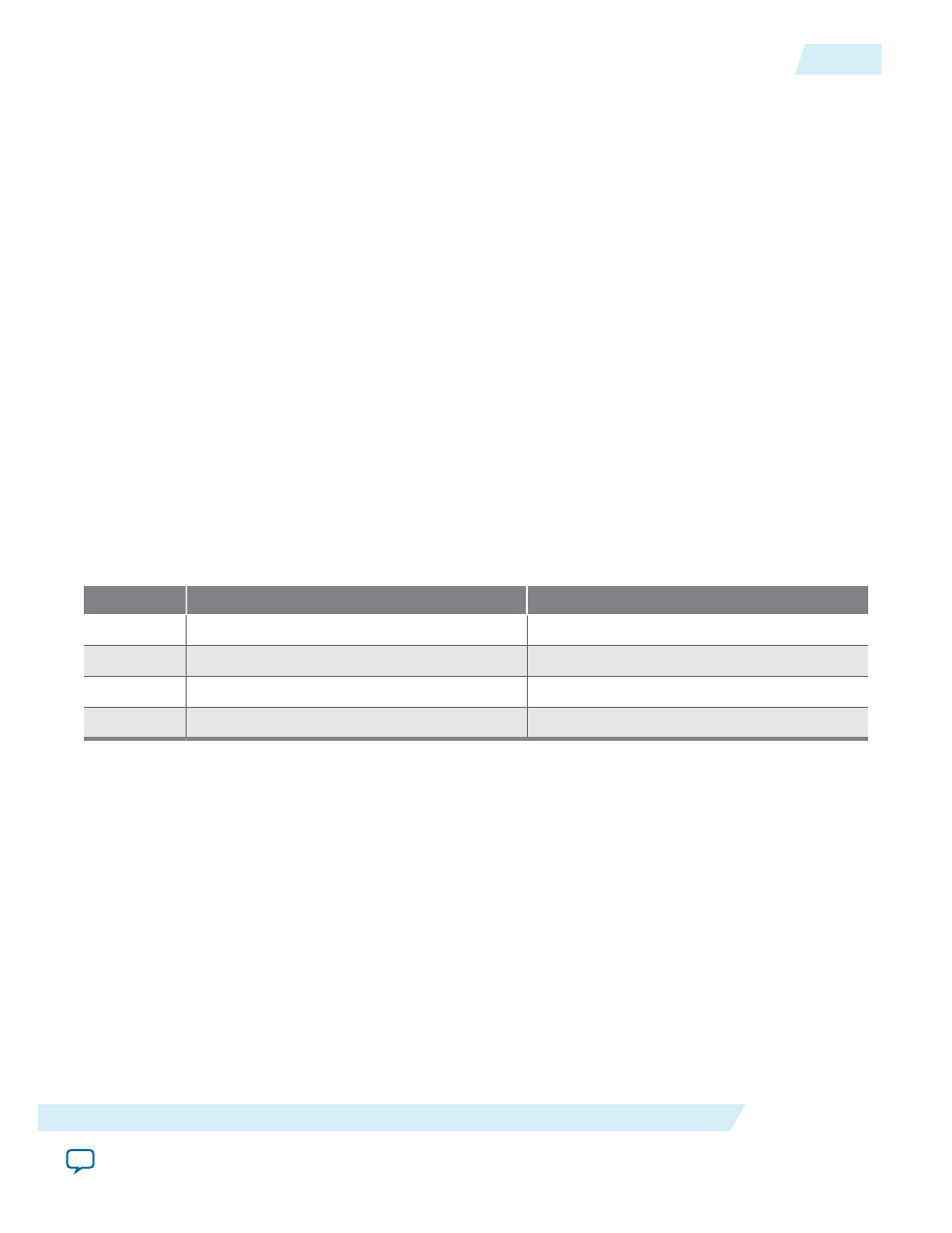
Table 5-3: txframe_clk and rxframe_clk Frequency for Different F Parameter Settings
For a given f
txlink
(txlink_clk frequency) and f
rxlink
(rxlink_clk frequency), the f
txframe
(txframe_clk frequency) and
f
rxframe
(rxframe_clk frequency) are derived from the formula listed in this table.
F Parameter
f
txframe
(txframe_clk frequency)
f
rxframe
(rxframe_clk frequency)
1
f
txlink
x (4 /
F1_FRAMECLK_DIV
)
f
rxlink
x (4 /
F1_FRAMECLK_DIV
)
2
f
txlink
x (2 /
F2_FRAMECLK_DIV
)
f
rxlink
x (2 /
F2_FRAMECLK_DIV
)
4
f
txlink
f
rxlink
8
f
txlink
/ 2
f
rxlink
/ 2
Data Bit and Content Mapping Scheme
One major function of the transport layer is to arrange the data bits in a specific way between the Avalon-
ST interface and the DLL in the JESD204B IP core.
shows the mapping scheme in the transport layer across various TX to RX interfaces for a
specific system configuration.
UG-01142
2015.05.04
Relationship Between Frame Clock and Link Clock
5-9
JESD204B IP Core Design Guidelines
Altera Corporation