Receiver, Receiver -36 – Altera JESD204B IP User Manual
Page 73
Receiver
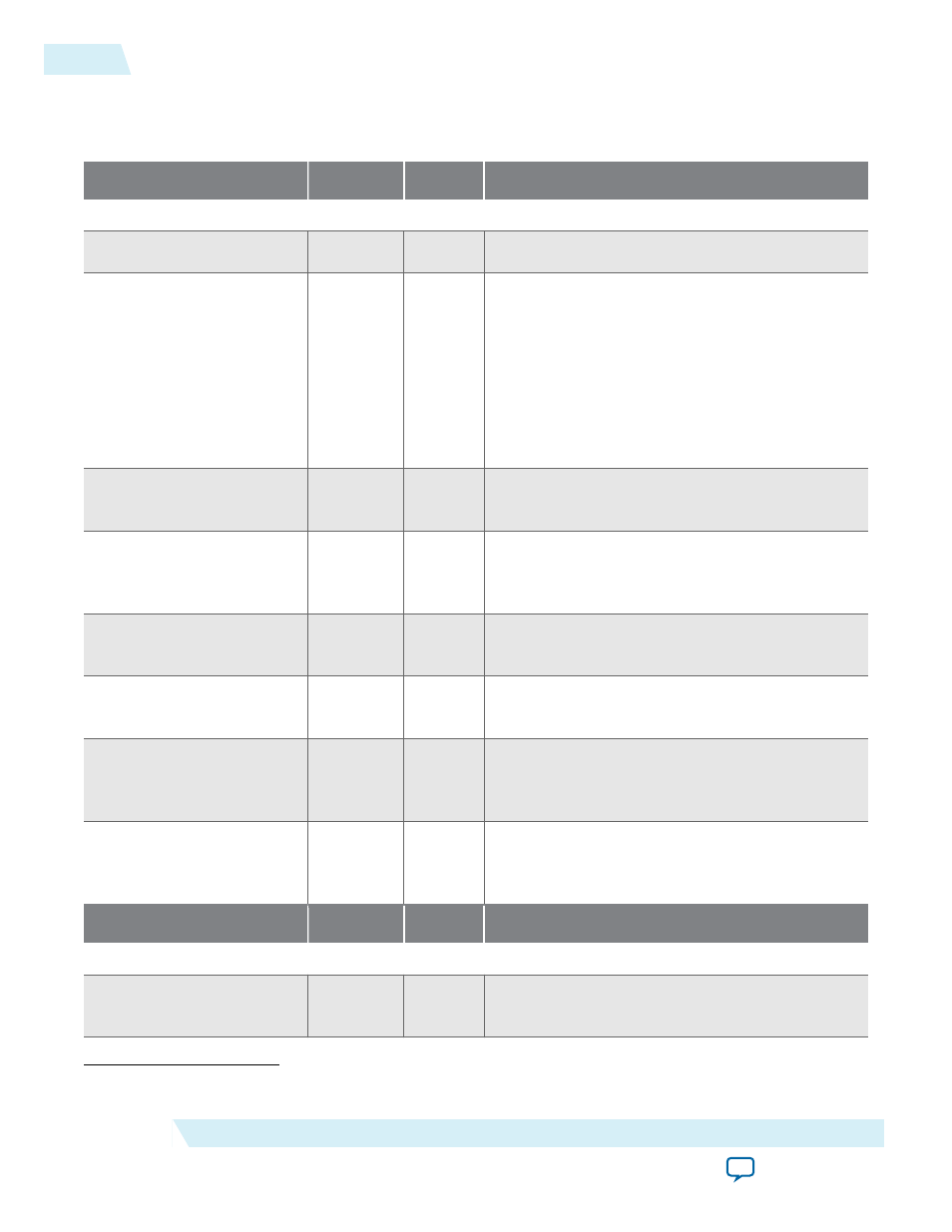
Table 4-6: Receiver Signals
Signal
Width
Direction
Description
Clocks and Resets
pll_ref_clk
1
Input
Transceiver reference clock signal.
rxlink_clk
1
Input
RX link clock signal used by the Avalon-ST
interface. This clock is equal to RX data rate
divided by 40.
For Subclass 1, you cannot use the output of
rxphy_clk
signal as
rxlink_clk
signal. To sample
SYSREF correctly, the core PLL must provide the
rxlink_clk
signal and must be configured as
normal operating mode.
rxlink_rst_n_reset_n
1
Input
Reset for the RX link clock signal. This reset is an
active low signal.
rxphy_clk[]
L
Output
Recovered clock signal. This clock is derived from
the clock data recovery (CDR) and the frequency
depends on the JESD204B IP core data rate.
rx_digitalreset[]
(25)
L
Input
Reset for the transceiver PCS block. This reset is an
active high signal.
rx_analogreset[]
(25)
L
Input
Reset for the CDR and transceiver PMA block.
This reset is an active high signal.
rx_islockedtodata[]
(25)
L
Output
This signal is asserted to indicate that the RX CDR
PLL is locked to the RX data and the RX CDR has
changed from LTR to LTD mode.
rx_cal_busy[]
(25)
L
Output
RX calibration in progress signal. This signal is
asserted to indicate that the RX transceiver calibra‐
tion is in progress.
Signal
Width
Direction
Description
Transceiver Interface
rx_serial_data[]
L
Input
Differential high speed serial input data. The clock
is recovered from the serial data stream.
(25)
The Transceiver PHY Reset Controller IP Core controls this signal.
4-36
Receiver
UG-01142
2015.05.04
Altera Corporation
JESD204B IP Core Functional Description