Altera JESD204B IP User Manual
Page 65
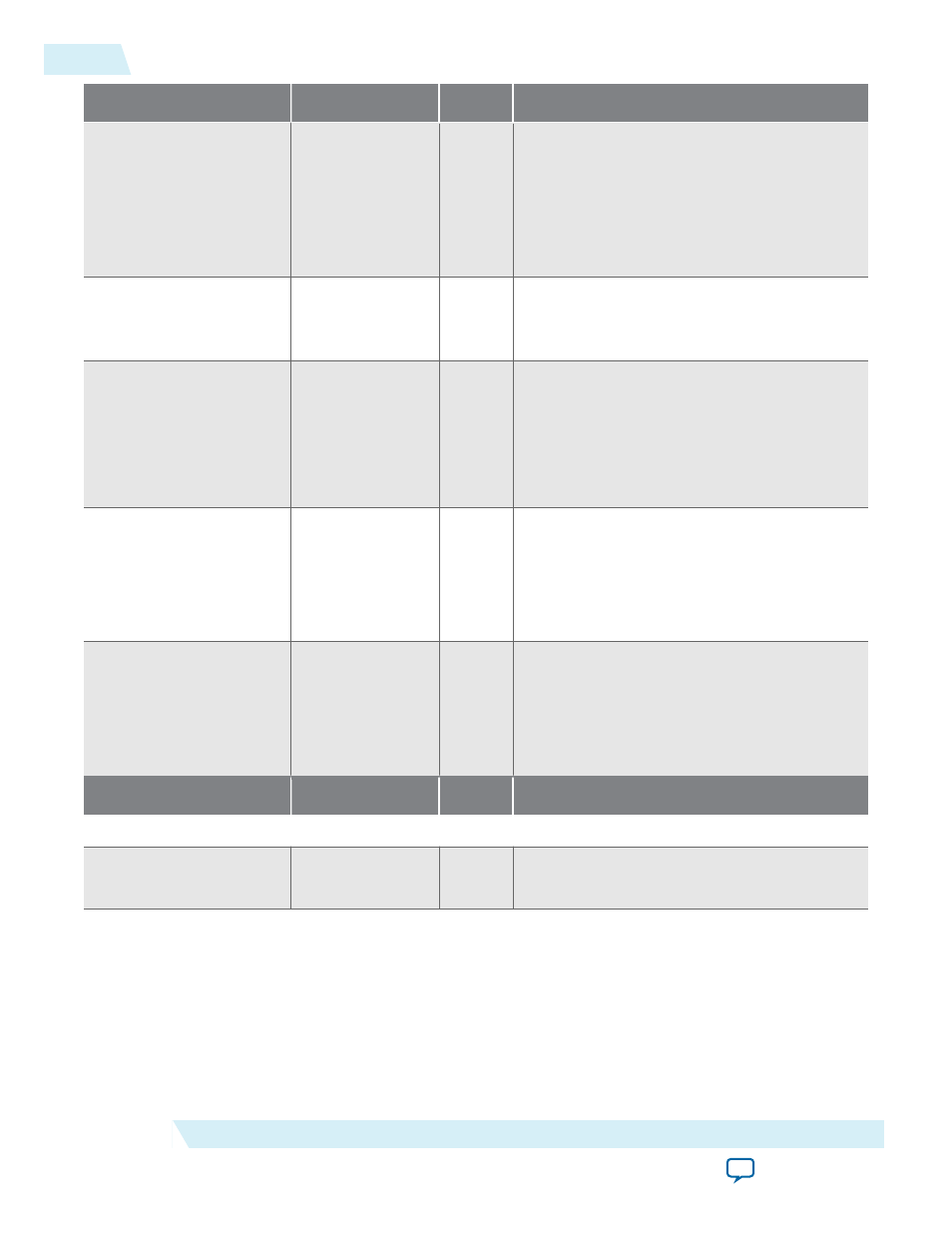
Signal
Width
Direction
Description
pll_locked[]
(22)
L
Output
PLL locked signal for the hard transceiver.
This signal is asserted to indicate that the TX
transceiver PLL is locked.
This signal is an output signal for V series
FPGA variants but an input signal for 10 series
FPGA variants and above.
tx_cal_busy[]
(22)
L
Output
TX calibration in progress signal. This signal is
asserted to indicate that the TX transceiver
calibration is in progress.
pll_powerdown[]
(22)
• 1 if bonding
mode = "xN"
• L if bonding
mode =
feedback_
compensation
Input
TX transceiver PLL power down signal.
This signal is only applicable for V series
FPGA variants.
tx_bonding_clocks
(Single Channel)
tx_bonding_clocks_
ch<0..L-1>
(Multiple
Channels)
6
Input
The transceiver PLL bonding clocks. The
transceiver PLL generation provides these
clocks.
This signal is only available if you select
Bonded mode for Arria 10 FPGA variants.
tx_serial_clk0
(Single
Channel)
tx_serial_clk0_
ch<0..L-1>
(Multiple
Channels)
1
Input
The transceiver PLL serial clock. This is the
serializer clock in the PMA. The transceiver
PLL generation provides these clocks.
This signal is only available if you select Non-
bonded mode for Arria 10 FPGA variants.
Signal
Width
Direction
Description
Transceiver Interface
tx_serial_data[]
L
Output
Differential high speed serial output data. The
clock is embedded in the serial data stream.
4-28
Transmitter
UG-01142
2015.05.04
Altera Corporation
JESD204B IP Core Functional Description