Altera JESD204B IP User Manual
Page 93
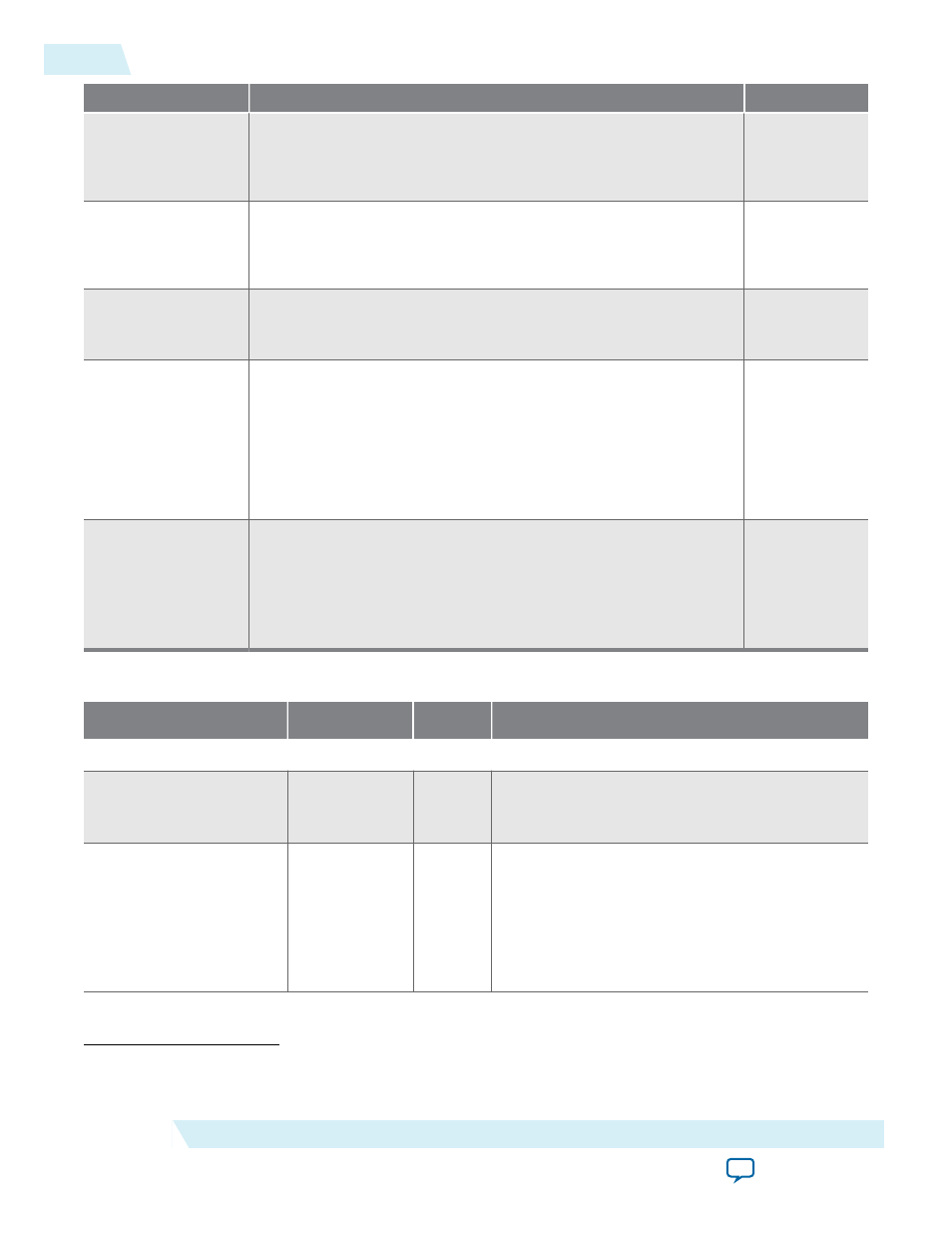
Parameter
Description
Value
F1_FRAMECLK_
DIV
Only applies to cases where F=1.
The divider ratio on the
frame_clk
. The assembler always use the
post-divided frame_clk (txframe_clk).
(29)
1, 4
F2_FRAMECLK_
DIV
Only applies to cases where F=2.
The divider ratio on the
frame_clk
. The assembler always use the
post-divided frame_clk (txframe_clk).
(29)
1, 2
RECONFIG_EN
Enable reconfiguration support in the transport layer. Only
downscaling reconfiguration is supported. Disable the reconfiguration
to reduce the logic.
0, 1
DATA_BUS_
WIDTH
The data input bus width size that depends on the F and L.
bus_width = M*S*N
F = (M*S*N_PRIME)/(8*L)
M*S = (8*F*L)/N_PRIME
Therefore the data bus width = (8*F*L*N)/N_PRIME
(8*F*L*N)/
N_PRIME
CONTROL_BUS_
WIDTH
The control output bus width size. The width depends on the CS
parameter as well as the M and S parameters. When CS is 0, the
control data is one bit wide (tie the signal to 0).
If CS = 0, the bus width = 1. Otherwise, the bus width = (OUTPUT_
BUS_WIDTH/N*CS) while OUTPUT_BUS_WIDTH/N = M*S
OUTPUT_
BUS_
WIDTH/
N*CS
Table 5-5: Assembler Signals
Signal
Clock Domain
Direction
Description
Control Unit
txlink_clk
—
Input
TX link clock signal. This clock is equal to the TX
data rate divided by 40. This clock is synchronous
to the
txframe_clk
signal.
txframe_clk
—
Input
TX frame clock used by the transport layer. The
frequency is a function of parameters F, F1_
FRAMECLK_DIV, F2_FRAMECLK_DIV and
txlink_clk.
This clock is synchronous to the
txlink_clk
signal.
(29)
Refer to the
to set the desired frame clock frequency with different FRAMECLK_DIV and F
values.
5-12
TX Path
UG-01142
2015.05.04
Altera Corporation
JESD204B IP Core Design Guidelines