Altera JESD204B IP User Manual
Page 36
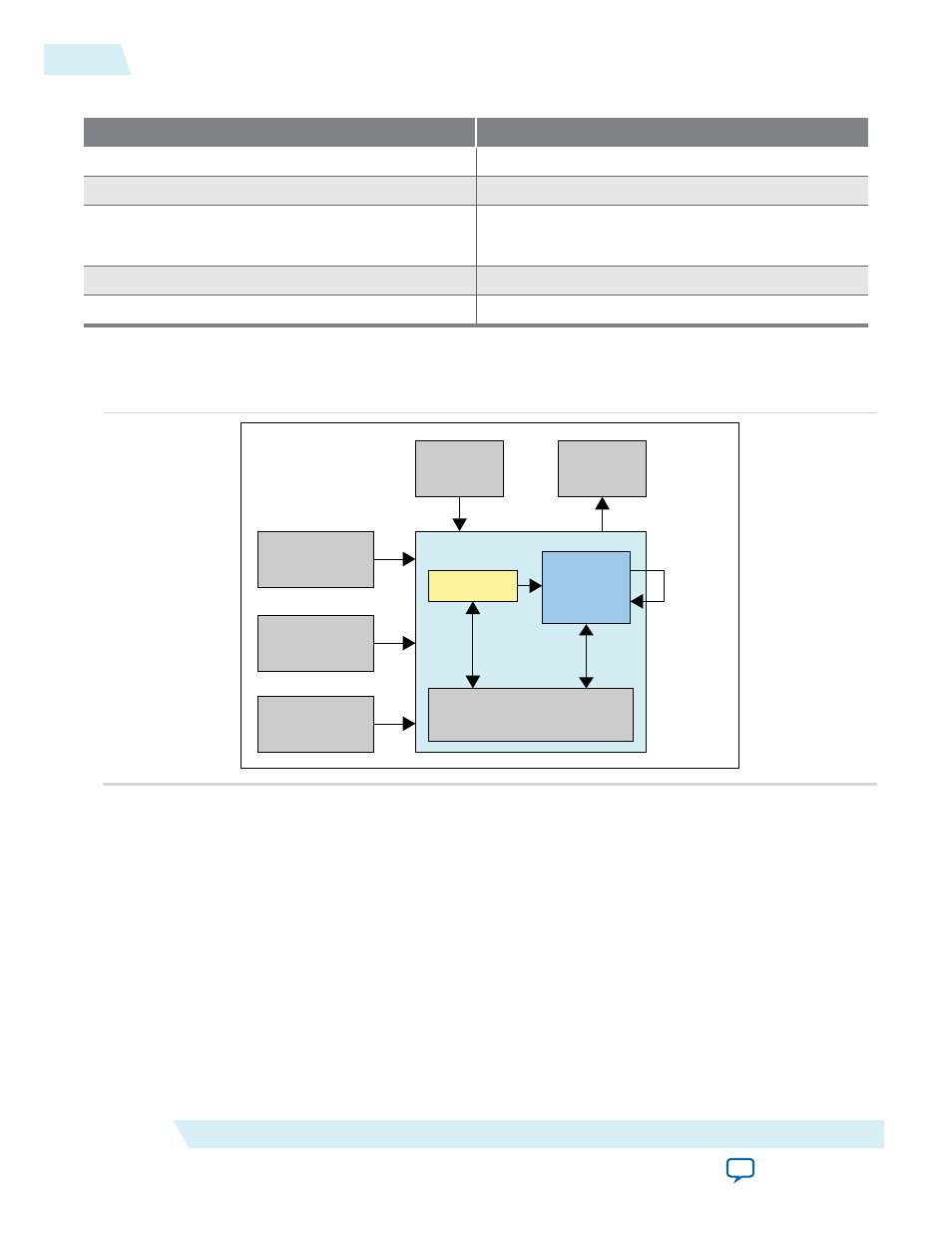
Table 3-8: Preset Configurations for JESD204B IP Core Testbench
Configuration
Preset Value
JESD204B Wrapper
Base and PHY (MAC and PHY)
Data Path
Duplex
PLL/CDR Reference Clock Frequency
• data_rate/20 (if you turn on Enabled Hard PCS)
• data_rate/40 (if you turn on Enabled Soft PCS)
Link Clock
Data rate/40
AVS Clock
125 MHz
Figure 3-5: JESD204B IP Core Testbench Block Diagram
The external ATX PLL is present only in the JESD204B IP core testbench targeting an Arria 10 FPGA
device family.
Reference Clock
Generator
Link Clock
Generator
AVS Clock
Generator
Packet
Generator
Packet
Checker
ATX PLL
Transceiver PHY Reset Controller
IP Core
JESD204B
IP Core
(Duplex)
Loopback
JESD204B Testbench
Related Information
Generating and Simulating the IP Core Testbench
3-22
JESD204B IP Core Testbench
UG-01142
2015.05.04
Altera Corporation
Getting Started