Altera JESD204B IP User Manual
Page 94
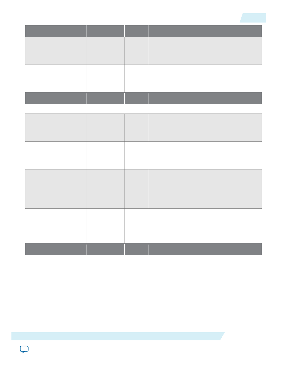
Signal
Clock Domain
Direction
Description
txlink_rst_n
txlink_clk
Input
Reset for the TX link clock domain logic in the
assembler. This reset is an active low signal and
the deassertion is synchronous to the rising-edge
of
txlink_clk
.
txframe_rst_n
txframe_clk
Input
Reset for the TX frame clock domain logic in the
assembler. This reset is an active low signal and
the deassertion is synchronous to the rising-edge
of
txframe_clk
.
Signal
Clock Domain
Direction
Description
Between Avalon- ST and Transport Layer
jesd204_tx_
datain[(DATA_BUS_
WIDTH)-1:0]
txframe_clk
Input
TX data from the Avalon-ST source interface.
The source shall arrange the data in a specific
order, as illustrated in the cases listed in
jesd204_tx_
controlin[(CONTROL_
BUS_WIDTH)-1:0]
txframe_clk
Input
TX control data from the Avalon-ST source
interface. The source shall arrange the data in a
specific order, as illustrated in the cases listed in
section
jesd204_tx_data_
valid
txframe_clk
Input
Indicates whether the data from the Avalon-ST
source interface to the transport layer is valid or
invalid.
• 0—data is invalid
• 1—data is valid
jesd204_tx_data_
ready
txlink_clk
Output
Indicates that the transport layer is ready to
accept data from the Avalon-ST source interface.
• 0—transport layer is not ready to receive data
• 1—transport layer is ready to receive data
Signal
Clock Domain
Direction
Description
Between Transport Layer and DLL
UG-01142
2015.05.04
TX Path
5-13
JESD204B IP Core Design Guidelines
Altera Corporation