2 rmii example schematic, Rmii example schematic, Table 40: rmii interface signals – BECKHOFF EtherCAT IP Core for Altera FPGAs v3.0.10 User Manual
Page 94: Figure 30: rmii example schematic
Ethernet Interface
III-82
Slave Controller
– IP Core for Altera FPGAs
Table 40: RMII Interface signals
Signal
Direction
Description
CLK50
IN
RMII RX/TX reference clock (50 MHz)
nRMII_LINK
IN
Input signal provided by the PHY if a 100 Mbit/s (Full
Duplex) link is established (alias LINK_MII)
RMII_RX_DV
IN
Carrier sense/receive data valid
RMII_RX_DATA[1:0]
IN
Receive data (alias RXD)
RMII_RX_ERR
IN
Receive error (alias RX_ER)
RMII_TX_ENA
OUT
Transmit enable (alias TX_EN)
RMII_TX_DATA[1:0]
OUT
Transmit data (alias TXD)
NPHY_RESET_OUT
OUT
PHY reset (akt. Low), resets PHY while ESC is in
Reset state, and, for FX PHYs, if Enhanced Link
Detection detects a lost link
NOTE: A pull-down resistor is typically required for NPHY_RESET_OUT to hold the PHY in reset state while the
FPGA is configured, since this pin is floating or even pulled up during that time.
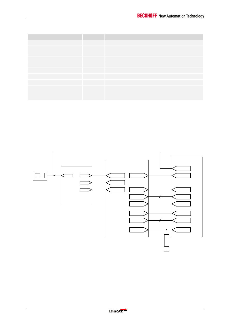
9.3.2
RMII example schematic
Refer to chapter 8.5 for more information on special markings (!). Take care of proper PHY address
configuration.
EtherCAT IP Core
Ethernet PHY
RMII_RX_DV
RMII_RX_DATA[1:0]
RMII_RX_ERR
RMII_TX_ENA
RMII_TX_DATA[1:0]
CRS_DV
RXD[1:0]
RX_ER
TX_EN
TXD[1:0]
REF_CLK
nRMII_LINK
LINK_STATUS
!
CLK25
PLL
CLK_IN
CLK25
CLK100
CLK100
50 MHz
CLK50
CLK50
NPHY_RESET_OUT
NRESET
4
K
7
Figure 30: RMII example schematic