Steps in creating a design for pci express – Altera Arria V Avalon-ST User Manual
Page 12
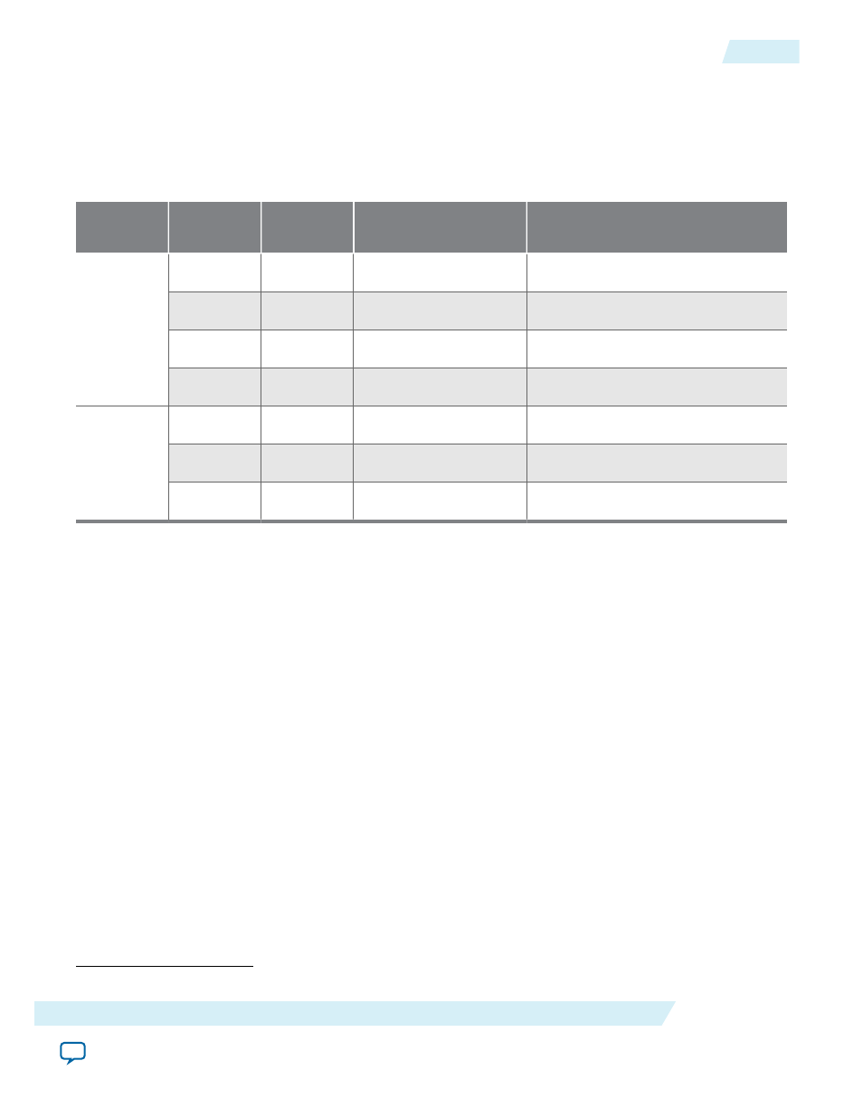
Table 1-5: Arria V Recommended Speed Grades for Link Widths and Application Layer Clock Frequencies
Altera recommends setting the Quartus II Analysis & Synthesis Settings Optimization Technique to Speed when
the Application Layer clock frequency is 250 MHz. For information about optimizing synthesis, refer to Setting Up
and Running Analysis and Synthesis in Quartus II Help. For more information about how to effect the
Optimization Technique settings, refer to Area and Timing Optimization in volume 2 of the Quartus II
Handbook. .
Link Rate
Link Width
Interface
Width
Application Clock
Frequency (MHz)
Recommended Speed Grades
Gen1
×1
64 bits
62.5
(2)
,125
–4,–5,–6
×2
64 bits
125
–4,–5,–6
×4
64 bits
125
–4,–5,–6
×8
128 bits
125
–4,–5,–6
Gen2
×1
64 bits
125
–4,–5
×2
64 bits
125
–4,–5
×4
128 bits
125
–4,–5
Related Information
•
•
•
Steps in Creating a Design for PCI Express
Before you begin
Select the PCIe variant that best meets your design requirements.
• Is your design an Endpoint or Root Port?
• What Generation do you intend to implement?
• What link width do you intend to implement?
• What bandwidth does your application require?
• Does your design require CvP?
1. Select parameters for that variant.
2. Simulate using an Altera-provided example design. All of Altera's PCI Express example designs are
available under
<install_dir>/ip/altera/altera_pcie/
. Alternatively, create a simulation model and use your
own custom or third-party BFM. The Qsys Generate menu generates simulation models. Altera
(2)
This is a power-saving mode of operation
2014.12.15
Steps in Creating a Design for PCI Express
1-11
Datasheet
Altera Corporation