Clock signals, Reset signals – Altera Arria V Avalon-ST User Manual
Page 61
Clock Signals
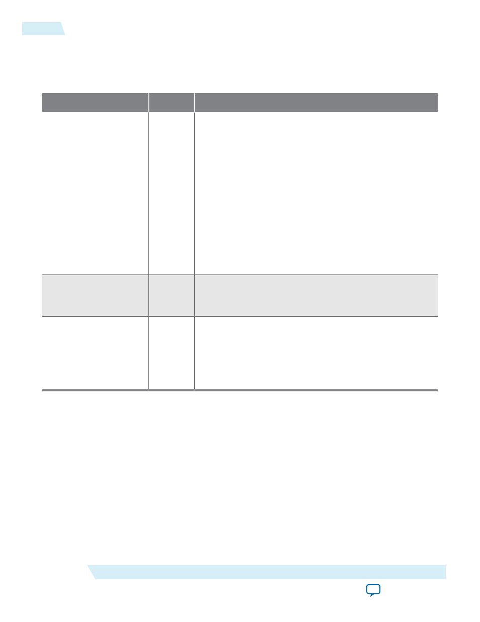
Table 4-5: Clock Signals
Signal
Direction
Description
refclk
Input
Reference clock for the IP core. It must have the frequency
specified under the System Settings heading in the parameter
editor. This is a dedicated free running input clock to the
dedicated
REFCLK
pin.
If your design meets the following criteria:
• Enables CvP
• Includes an additional transceiver PHY connected to the same
Transceiver Reconfiguration Controller
then you must connect
refclk
to the
mgmt_clk_clk
signal of the
Transceiver Reconfiguration Controller and the additional
transceiver PHY. In addition, if your design includes more than
one Transceiver Reconfiguration Controller on the same side of
the FPGA, they all must share the
mgmt_clk_clk
signal.
pld_clk
Input
Clocks the Application Layer. You can drive this clock with
coreclkout_hip
. If you drive
pld_clk
with another clock
source, it must be equal to or faster than
coreclkout_hip
.
coreclkout
Output
This is a fixed frequency clock used by the Data Link and
Transaction Layers. To meet PCI Express link bandwidth
constraints, this clock has minimum frequency requirements as
listed in Application Layer Clock Frequency for All Combination
of Link Width, Data Rate and Application Layer Interface Width
in the Reset and Clocks chapter .
Related Information
on page 6-5
Reset Signals
Refer to Reset and Clocks for more information about the reset sequence and a block diagram of the reset
logic.
4-24
Clock Signals
2014.12.15
Altera Corporation
Interfaces and Signal Descriptions